Nitrogen-vacancy center
[6] NV centers enable nanoscale measurements of magnetic and electric fields, temperature, and mechanical strain with improved precision.
External perturbation sensitivity makes NV centers ideal for applications in biomedicine—such as single-molecule imaging and cellular process modeling.
This can be achieved by applying external voltage to a p-n junction made from doped diamond, e.g., in a Schottky diode.
[12] A wide range of high-energy particles is suitable for such irradiation, including electrons, protons, neutrons, ions, and gamma photons.
During chemical vapor deposition of diamond, a small fraction of single substitutional nitrogen impurity (typically <0.5%) traps vacancies generated as a result of the plasma synthesis.
[26][27] Delta doping of nitrogen during CVD growth can be used to create two-dimensional ensembles of NV centers near the diamond surface for enhanced sensing[28] or simulation.
[41] It was not this structure alone, but a combination of several favorable factors (previous knowledge, easy production, biocompatibility, simple initialisation, use at room temperature etc.)
At room temperature the NV center's optical spectrum exhibits no sharp peaks due to thermal broadening.
Specifically, transitions between the ground and excited states (with equal spin) can be induced using a green laser with a wavelength of 546 nm.
[62] There are inherent difficulties in achieving miniaturization and effective error reduction in microwave and radio frequency driven spin manipulation techniques.
This poses special challenge on application of spin based quantum sensors on sensing electric and magnetic field or any physical phenomena at nanoscale level.
The recent developments in microwave-free and optically driven methods[63][64] pave the way towards energy efficient and coherent quantum sensing.
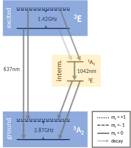
[65] There is an additional splitting of the ms = ±1 energy levels, which originates from the hyperfine interaction between surrounding nuclear spins and the NV center.
Also the NV center's own spin–orbit interaction and orbital degeneracy leads to additional level splitting in the excited 3E state.
Temperature and pressure directly influence the zero-field term of the NV center leading to a shift between the ground and excited state levels.
The Hamiltonian, a quantum mechanical equation describing the dynamics of a system, which shows the influence of different factors on the NV center can be found below.
In a similar capacity, nitrogen termination also affects surface properties and can optimize NV centers for specific sensing applications.
[68] The spectral shape and intensity of the optical signals from the NV− centers are sensitive to external perturbation, such as temperature, strain, electric and magnetic field.
However, the use of spectral shape for sensing those perturbation is impractical, as the diamond would have to be cooled to cryogenic temperatures to sharpen the NV− signals.
A more realistic approach is to use luminescence intensity (rather than lineshape), which exhibits a sharp resonance when a microwave frequency is applied to diamond that matches the splitting of the ground-state levels.
The resulting optically detected magnetic resonance signals are sharp even at room temperature, and can be used in miniature sensors.
This sensitivity allows detecting a magnetic or electric field produced by a single electron located tens of nanometers away from an NV− center.
[78] In addition to the quantum optical applications, luminescence from the NV− centers can be applied for imaging biological processes, such as fluid flow in living cells.
[79][80] This application relies on good compatibility of diamond nano-particles with the living cells and on favorable properties of photoluminescence from the NV− centers (strong intensity, easy excitation and detection, temporal stability, etc.).
NV− centers are produced in diamond powders with sub-micrometre particle size using the standard process of irradiation and annealing described above.
This method reduces the required ion dose and reaction, making it possible to mass-produce fluorescent nanodiamonds in ordinary laboratory.
[81] Fluorescent nanodiamond produced with such method is bright and photostable, making it excellent for long-term, three dimensional tracking of single particle in living cell.
[85][86] It used 532-nm pumped NV− centers held within a high Purcell factor microwave cavity and an external magnetic field of 4300 G. Continuous maser oscillation generated a coherent signal at ~9.2 GHz.
[89] Disadvantageous for these applications is the long radiative lifetime (~12 ns[90][91] ) of the NV center and the strong phonon sideband in its emission spectrum.
[35] The characterization of single NV− centers has become a very competitive field nowadays, with many dozens of papers published in the most prestigious scientific journals.


(a) Schematics of experimental setup. An electric current is applied to the arms of an AFM cantilever ( phosphorus -doped Si, P:Si) and heats up the end section above the tip ( intrinsic Si, i -Si). The bottom lens excites a diamond nanocrystal with a green laser light and collects photoluminescence (PL). The crystal hosts an NV center and is attached to the AFM tip. A wire on the sample surface serves as the microwave source (mw). The temperature of the cantilever T h is determined from the applied current and voltage.
(b) ODMR spectra of the NV center at three temperatures. The line splitting originates from a ~1 mT applied magnetic field.
(c) Thermal conductivity image of a gold letter E on sapphire . White circles indicate features that do not correlate with the AFM topography. (d) PL image of the AFM cantilever end and tip where the diamond nanocrystal appears as the bright spot. (e) Zoomed PL image of the NV center in d. [ 69 ]