Ferroelectric RAM
An FeRAM chip contains a thin film of ferroelectric material, often lead zirconate titanate, commonly referred to as PZT.
The atoms in the PZT layer change polarity in an electric field, thereby producing a power-efficient binary switch.
However, the most important aspect of the PZT is that it is not affected by power disruption or magnetic interference, making FeRAM a reliable nonvolatile memory.
[1] FeRAM's advantages over Flash include: lower power usage, faster write speeds[2] and a much greater maximum read/write endurance (about 1010 to 1015 cycles).
[6] Following the introduction of metal–oxide–semiconductor (MOS) dynamic random-access memory (DRAM) chips in the early 1970s,[7] development of FeRAM began in the late 1980s.
One major licensee is Fujitsu, who operates one of the largest semiconductor foundry production lines with FeRAM capability.
Since at least 2001 Texas Instruments has collaborated with Ramtron to develop FeRAM test chips in a modified 130 nm process.
A ferroelectric material has a nonlinear relationship between the applied electric field and the apparently stored charge.
If the cell held a "1", the re-orientation of the atoms in the film will cause a brief pulse of current in the output as they push electrons out of the metal on the "down" side.
For DRAM, this appears to be a problem at around 55 nm, at which point the charge stored in the capacitor is too small to be detected.
It is not clear whether FeRAM can scale to the same size, as the charge density of the PZT layer may not be the same as the metal plates in a normal capacitor.
There is ongoing research on addressing the problem of stabilizing ferroelectric materials; one approach, for example, uses molecular adsorbates.
Early models required two FeRAM cells per bit, leading to very low densities, but this limitation has since been removed.
In DRAM, the charge deposited on the metal plates leaks across the insulating layer and the control transistor, and disappears.
In order for a DRAM to store data for anything other than a very short time, every cell must be periodically read and then re-written, a process known as refresh.
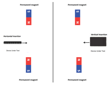
Data reliability is guaranteed in F-RAM even in a high magnetic field environment compared to MRAM.
In addition, the F-RAM devices allow rewriting with a different data pattern after exposure to the magnetic fields.
FeRAM is based on the physical movement of atoms in response to an external field, which is extremely fast, averaging about 1 ns.
Whereas the read operation is likely to be similar in speed, the charge pump used for writing requires a considerable time to "build up" current, a process that FeRAM does not need.
In 2005, Ramtron reported significant sales of its FeRAM products in a variety of sectors including (but not limited to) electricity meters,[24] automotive (e.g. black boxes, smart air bags), business machines (e.g. printers, RAID disk controllers), instrumentation, medical equipment, industrial microcontrollers, and radio frequency identification tags.
Texas Instruments proved it to be possible to embed FeRAM cells using two additional masking steps[citation needed] during conventional CMOS semiconductor manufacture.
Both the PZT ferroelectric layer and the noble metals used for electrodes raise CMOS process compatibility and contamination issues.