Front-side bus
Front-side buses usually connect the CPU and the rest of the hardware via a chipset, which Intel implemented as a northbridge and a southbridge.
These secondary system buses usually run at speeds derived from the front-side bus clock, but are not necessarily synchronized to it.
[5][6][7] The frequency at which a processor (CPU) operates is determined by applying a clock multiplier to the front-side bus (FSB) speed in some cases.
A slow FSB will cause the CPU to spend significant amounts of time waiting for data to arrive from system memory.
However, if the computations involving each element are more complex, the processor will spend longer performing these; therefore, the FSB will be able to keep pace because the rate at which the memory is accessed is reduced.
Most PCs purchased from retailers or manufacturers, such as Hewlett-Packard or Dell, do not allow the user to change the multiplier or FSB settings due to the probability of erratic behavior or failure.
Motherboards purchased separately to build a custom machine are more likely to allow the user to edit the multiplier and FSB settings in the PC's BIOS.
Simple symmetric multiprocessors place a number of CPUs on a shared FSB, though performance could not scale linearly due to bandwidth bottlenecks.
The front-side bus was used in all Intel Atom, Celeron, Pentium, Core 2, and Xeon processor models through about 2008[8] and was eliminated in 2009.
[10] More modern designs use point-to-point and serial connections like AMD's HyperTransport and Intel's DMI 2.0 or QuickPath Interconnect (QPI).
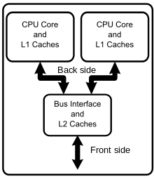
[11][12][13] In a traditional architecture, the front-side bus served as the immediate data link between the CPU and all other devices in the system, including main memory.
This increases the complexity of the CPU design but offers greater throughput as well as superior scaling in multiprocessor systems.
Many manufacturers publish the frequency of the front-side bus in MHz, but marketing materials often list the theoretical effective signaling rate (which is commonly called megatransfers per second or MT/s).