Heterojunction
It is often advantageous to engineer the electronic energy bands in many solid-state device applications, including semiconductor lasers, solar cells and transistors.
The combination of multiple heterojunctions together in a device is called a heterostructure, although the two terms are commonly used interchangeably.
Heterojunction manufacturing generally requires the use of molecular beam epitaxy (MBE)[1] or chemical vapor deposition (CVD) technologies in order to precisely control the deposition thickness and create a cleanly lattice-matched abrupt interface.
A recent alternative under research is the mechanical stacking of layered materials into van der Waals heterostructures.
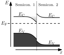
[2] Despite their expense, heterojunctions have found use in a variety of specialized applications where their unique characteristics are critical: The behaviour of a semiconductor junction depends crucially on the alignment of the energy bands at the interface.
[9] Away from the junction, the band bending can be computed based on the usual procedure of solving Poisson's equation.
In order to calculate the static energy levels within the achieved quantum well, understanding variation or mismatch of the effective mass across the heterojunction becomes substantial.
The quantum well defined in the heterojunction can be treated as a finite well potential with width of
According to them, the envelope function in a fabricated quantum well must satisfy a boundary condition which states that
even-parity solution can be gained from By taking derivative of (5) and multiplying both sides by
In this system the much larger band gap ZnS passivates the surface of the fluorescent CdSe core thereby increasing the quantum efficiency of the luminescence.
There is an added bonus of increased thermal stability due to the stronger bonds in the ZnS shell as suggested by its larger band gap.
Since CdSe and ZnS both grow in the zincblende crystal phase and are closely lattice matched, core shell growth is preferred.
In other systems or under different growth conditions it may be possible to grow anisotropic structures such as the one seen in the image on the right.
Consequently, engineering the conduction band offset is typically much easier with nanoscale heterojunctions.
For staggered (type II) offset nanoscale heterojunctions, photoinduced charge separation can occur since there the lowest energy state for holes may be on one side of the junction whereas the lowest energy for electrons is on the opposite side.
It has been suggested[18] that anisotropic staggered gap (type II) nanoscale heterojunctions may be used for photocatalysis, specifically for water splitting with solar energy.