Amorphous silicon
As a second-generation thin-film solar cell technology, amorphous silicon was once expected to become a major contributor in the fast-growing worldwide photovoltaic market, but has since lost its significance due to strong competition from conventional crystalline silicon cells and other thin-film technologies such as CdTe and CIGS.
[citation needed] Amorphous silicon is a preferred material for the thin film transistor (TFT) elements of liquid crystal displays (LCDs) and for x-ray imagers.
In crystalline silicon (c-Si) this tetrahedral structure continues over a large range, thus forming a well-ordered crystal lattice.
Hydrogenated amorphous silicon (a-Si:H) has a sufficiently low amount of defects to be used within devices such as solar photovoltaic cells, particularly in the protocrystalline growth regime.
[3] Several studies are found in the scientific literature, mainly investigating the effects of deposition parameters on electronic quality, but practical applications of amorphous silicon carbide in commercial devices are still lacking.
Hydrogenated amorphous silicon, a-Si:H, was first fabricated in 1969 by Chittick, Alexander and Sterling by deposition using a silane gas (SiH4) precursor.
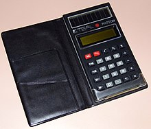
Hydrogenated amorphous silicon (a-Si:H) has been used as a photovoltaic solar cell material for devices which require very little power, such as pocket calculators, because their lower performance compared to conventional crystalline silicon (c-Si) solar cells is more than offset by their simplified and lower cost of deposition onto a substrate.
Moreover, the vastly higher shunt resistance of the p-i-n device means that acceptable performance is achieved even at very low light levels.
This approach is not applicable to c-Si cells, which are thick as a result of its indirect band-gap and are therefore largely opaque, blocking light from reaching other layers in a stack.
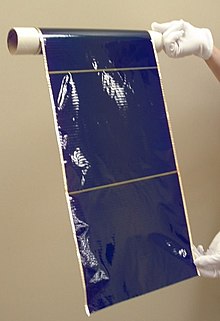
[18] However, the higher costs of manufacture due to the multi-layer construction have, to date, made a-Si:H unattractive except in roles where their thinness or flexibility are an advantage.
Uni-Solar, a division of Energy Conversion Devices produced a version of flexible backings, used in roll-on roofing products.
However, the world's largest manufacturer of amorphous silicon photovoltaics had to file for bankruptcy in 2012, as it could not compete with the rapidly declining prices of conventional solar panels.
Xunlight Corporation, which has received over $40 million of institutional investments,[citation needed] has completed the installation of its first 25 MW wide-web, roll-to-roll photovoltaic manufacturing equipment for the production of thin-film silicon PV modules.
[22] Anwell Technologies has also completed the installation of its first 40 MW a-Si thin film solar panel manufacturing facility in Henan with its in-house designed multi-substrate-multi-chamber PECVD equipment.
Amorphous silicon has become the material of choice for the active layer in thin-film transistors (TFTs), which are most widely used in large-area electronics applications, mainly for liquid-crystal displays (LCDs).
[24] Transistors take up only a small fraction of the area of each pixel and the rest of the silicon film is etched away to allow light to easily pass through it.