Atomic layer deposition
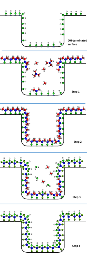
During atomic layer deposition, a film is grown on a substrate by exposing its surface to alternate gaseous species (typically referred to as precursors or reactants).
In contrast to chemical vapor deposition, the precursors are never present simultaneously in the reactor, but they are inserted as a series of sequential, non-overlapping pulses.
Consequently, the maximum amount of material deposited on the surface after a single exposure to all of the precursors (a so-called ALD cycle) is determined by the nature of the precursor-surface interaction.
[2][3] By varying the number of cycles it is possible to grow materials uniformly and with high precision on arbitrarily complex and large substrates.
A major driving force for the recent interest is the prospective seen for ALD in scaling down microelectronic devices according to Moore's law.
[5] Currently there are several comprehensive review papers that give a summary of the published ALD processes, including the work of Puurunen,[6] Miikkulainen et al.,[5] Knoops et al.,[7] and Mackus & Schneider et al..[8] An interactive, community driven database of ALD processes is also available online[4] which generates an up-to-date overview in the form of an annotated periodic table.
In the 1960s, Stanislav Koltsov together with Valentin Aleskovsky and colleagues experimentally developed the principles of ALD at Leningrad Technological Institute (LTI) in the Soviet Union.
[9] The experiments started with metal chloride reactions and water with porous silica, soon extending to other substrate materials and planar thin films.
In 1987, Suntola started the development of the ALE technology for new applications like photovoltaic devices and heterogeneous catalysts in Microchemistry Ltd., established for that purpose by the Finnish national oil company Neste Oy.
[11][9] An attempt to expose the extent of molecular layering works was made in a scientific ALD review article in 2005[3] and later in the VPHA-related publications.
[15][9][16] The name "atomic layer deposition" was apparently proposed for the first time in writing as an alternative to ALE in analogy with CVD by Markku Leskelä (professor at the University of Helsinki) at the ALE-1 conference, Espoo, Finland.
It took about a decade before the name gained general acceptance with the onset of the international conference series on ALD by American Vacuum Society.
[17] In 2000, Gurtej Singh Sandhu and Trung T. Doan of Micron Technology initiated the development of atomic layer deposition high-κ films for DRAM memory devices.
[15][11][9][16] In 2010, sequential infiltration synthesis (SIS), first reported by researchers at Argonne National Laboratory, was added to the family of ALD-derived techniques.
[26] It occurs through surface reactions, which enables accurate thickness control no matter the substrate geometry (subject to aspect ratio) and reactor design.
The chemistry for spatial ALD processes is comparable with typical temporal ALD processes, and materials that have been explored include inorganic metal oxides such as Al2O3, (Al- or Ga doped) ZnO, SiO2, In2O3, InZnO, LIPON, Zn(O,S), SnOx, and TiOx ,but also PMG metals (Pt, Ir, Ru) can be deposited.
Additionally, organic molecules can be grown in combination with inorganic atoms to enable molecular layer deposition (MLD).
Recently, the application of novel strong reducing agents has led to the first reports of low-temperature thermal ALD processes for several electropositive metals.
Similarly, hydrogen bonding between a Lewis base and an H2O reactant make the electronegative O in H2O a strong nucleophile that is able to attack the Si in an existing SiCl* surface species.
ALD is a useful process for the fabrication of microelectronics due to its ability to produce accurate thicknesses and uniform surfaces in addition to high quality film production using various different materials.
In dynamic random access memories (DRAMs), the conformality requirements are even higher and ALD is the only method that can be used when feature sizes become smaller than 100 nm.
Several products that use ALD include magnetic recording heads, MOSFET gate stacks, DRAM capacitors, nonvolatile ferroelectric memories, and many others.
The motivation for high-κ oxides comes from the problem of high tunneling current through the commonly used SiO2 gate dielectric in MOSFETs when it is downscaled to a thickness of 1.0 nm and below.
With the high-κ oxide, a thicker gate dielectric can be made for the required capacitance density, thus the tunneling current can be reduced through the structure.
[56] The use of ALD technique to deposit charge transport layers (CTLs) is also being explored widely for perovskite solar cells.
The ability of ALD to deposit high quality and conformal films with precise control on thickness can provide great advantage in finely tailoring the interfaces between CTL and perovskite layer.
One example is the nanophotonic coupler that behaves as a micrometer-size beamsplitter at the intersection of optical waveguides[58] in which high aspect ratio trenches (~100 nm width x 4 micrometer depth) are first defined by etching then back-filled with aluminum oxide by ALD to form optical-quality interfaces.
[60] Also, ALD is beneficial in creating flexible sensing devices that can be used, for example, in the clothing of athletes to detect movement or heart rate.
[64][65] ALD can also be used to inoculate 3-D printed plastic parts for use in vacuum environments by mitigating outgassing, which allows for custom low-cost tools for both semiconductor processing and space applications.
X-ray reflectivity (XRR) is a technique that measures thin-film properties including thickness, density, and surface roughness.