Kikuchi lines (physics)
They pair up to form bands in electron diffraction from single crystal specimens, there to serve as "roads in orientation-space" for microscopists uncertain of what they are looking at.
Kikuchi band intersections, or zones, on the other hand are indexed with direct-lattice indices i.e. indices which represent integer multiples of the lattice basis vectors a, b and c. Kikuchi lines are formed in diffraction patterns by diffusely scattered electrons, e.g. as a result of thermal atom vibrations.
[3] The main features of their geometry can be deduced from a simple elastic mechanism proposed in 1928 by Seishi Kikuchi,[4] although the dynamical theory of diffuse inelastic scattering is needed to understand them quantitatively.
Fully quantitative work on such diffraction features is therefore assisted by the large linear dynamic range of CCD detectors.
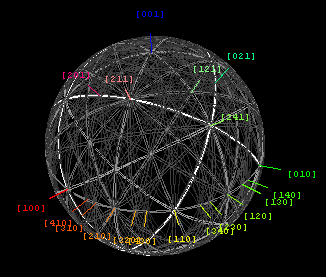
Such conformal projections allow one to map pieces of spherical surface onto a plane while preserving the local angles of intersection, and hence zone symmetries.
Finding a beam compass today might be fairly difficult, since it is much easier to draw curves having a large radius of curvature (in two or three dimensions) with help from a computer.
The angle-preserving effect of stereographic plots is even more obvious in the figure at right, which subtends a full 180° of the orientation space of a face-centered or cubic close packed crystal e.g. like that of Gold or Aluminum.
Kikuchi lines serve to highlight the edge on lattice planes in diffraction images of thicker specimens.
Because Bragg angles in the diffraction of high energy electrons are very small (~1⁄4 degrees for 300 keV), Kikuchi bands are quite narrow in reciprocal space.
As this angle changes in either direction from edge-on (at which orientation the electron beam runs parallel to the lattice planes and perpendicular to their normal), the beam moves into Bragg diffracting condition and more electrons are diffracted outside the microscope's back focal plane aperture, giving rise to the dark-line pairs (bands) seen in the image of the bent silicon foil shown in the image on the right.
[13] However, practical uses for the technique are limited because only a thin layer of abrasion damage or amorphous coating is generally adequate to obscure the contrast.