MEMS for in situ mechanical characterization
Furthermore, analytical capabilities of these instruments such as spectroscopy and diffraction can be used to further characterize the sample, providing a complete picture of the evolution of the specimen as it is loaded and fails.
Likewise, Horacio D. Espinosa at Northwestern University developed a membrane deflection experiment,[3] which was employed at the MEMS level[4] as well as in thin film specimens.
[5] Later, size effect studies were performed on single crystal pillars using nanoindentation of microfabricated samples by means of focused ion beam.
[6] Several results in situ SEM and TEM were demonstrated for thin films by his group[7] including a stage for simultaneous electrical and mechanical testing, although this set-up used external actuation and sensing.
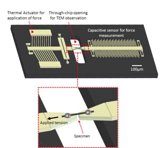
They designed and developed a true MEM system that incorporated capacitive sensing for electronic measurement of load and thermal actuation for specimen straining in one single chip.
The MEMS based platform was applied to the study of poly-Silicon samples,[10] multi-walled CNTs[11] and more recently metallic[10] and semiconducting nanowires.
[14] At the Ecole Polythecnique Federale de Lausanne (EPFL), an electrostatically actuated device, similar to Espinosa’s original design, was developed in Silicon-On-Insulator technology by the Michler’s group.
Some other researchers have developed other devices following the models outlines by Espinosa, Saif and Haque; for example Victor Bright at University of Colorado – Boulder.
[16] The technology has reached a level of maturity such that standard devices are now offered by the Center for Integrated Nanotechnologies (CINT) at Sandia National Labs to researchers interested in mechanical testing of nanoscale samples.