Nanorod
A combination of ligands act as shape control agents and bond to different facets of the nanorod with different strengths.
Nanorods based on semiconducting materials have also been investigated for application as energy harvesting and light emitting devices.
In 2006, Ramanathan et al. demonstrated1 electric-field mediated tunable photoluminescence from ZnO nanorods, with potential for application as novel sources of near-ultraviolet radiation.
Apart from these manufacturing schemes, ZnO nanorods and tubes can be fabricated by the combination of deep UV lithography, dry etch, and atomic layer deposition (ALD).
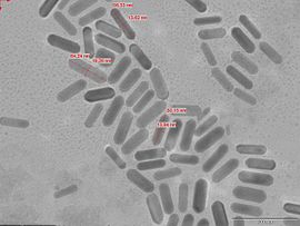
The growth solution is obtained by the reduction of HAuCl4 with ascorbic acid in the presence of cetyltrimethylammonium bromide (CTAB) surfactant and silver ions.
Longer nanorods (up to an aspect ratio of 25) can be obtained in the absence of silver nitrate by use of a three-step addition procedure.
In one modifications of this method sodium citrate is replaced with a stronger CTAB stabilizer in the nucleation and growth procedures.
[11] Another improvement is to introduce silver ions to the growth solution, which results in the nanorods of aspect ratios less than five in greater than 90% yield.
[12] Silver, of a lower reduction potential than gold, can be reduced on the surface of the rods to form a monolayer by underpotential deposition.
Polymers, such as Polyethylene glycol (PEG), Polyallylamine hydrochloride (PAH) coating; dietary fibers, such as chitosan; or biomolecules, such as phospholipids have been used to displace the CTAB out from the nanorod surface without affecting the stability has been reported.
Compared to bulk crystal systems, the cation exchange of nanorods is million-times faster due to high surface area.