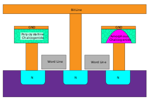
Phase-change memory
In 1969, Charles Sie published a dissertation at Iowa State University that both described and demonstrated the feasibility of a phase-change-memory device by integrating chalcogenide film with a diode array.
More recently, interest and research have resumed as flash and DRAM memory technologies are expected to encounter scaling difficulties as chip lithography shrinks.
However, a January 2006 Samsung Electronics patent application indicates PRAM may achieve switching times as fast as five nanoseconds.
Each of these states has different electrical properties that can be measured during reads, allowing a single cell to represent two bits, doubling memory density.
PRAM's temperature sensitivity is perhaps its most notable drawback, one that may require changes in the production process of manufacturers incorporating the technology.
Changing the bit's state requires removing the accumulated charge, which demands a relatively large voltage to "suck" the electrons off the floating gate.
The special gates used in flash memory "leak" charge (electrons) over time, causing corruption and loss of data.
The resistivity of the memory element in PRAM is more stable; at the normal working temperature of 85 °C, it is projected to retain data for 300 years.
[citation needed] Because flash devices trap electrons to store information, they are susceptible to data corruption from radiation, making them unsuitable for many space and military applications.
Thin film-based selectors allow higher densities, utilizing < 4 F2 cell area by stacking memory layers horizontally or vertically.
Often the isolation capabilities are inferior to the use of transistors if the on/off ratio for the selector is not sufficient, limiting the ability to operate very large arrays in this architecture.
Chalcogenide-based threshold switches have been demonstrated as a viable selector for high-density PCM arrays [22] In August 2004, Nanochip licensed PRAM technology for use in MEMS (micro-electric-mechanical-systems) probe storage devices.
PRAM is also a promising technology in the military and aerospace industries where radiation effects make the use of standard non-volatile memories such as flash impractical.
PRAM devices have been introduced by BAE Systems, referred to as C-RAM, claiming excellent radiation tolerance (rad-hard) and latchup immunity.
In addition, BAE claims a write cycle endurance of 108, which will allow it to be a contender for replacing PROMs and EEPROMs in space systems.
This means that instead of the normal two states—fully amorphous and fully crystalline—an additional two distinct intermediate states represent different degrees of partial crystallization, allowing for twice as many bits to be stored in the same physical area.
[16] In June 2011,[25] IBM announced that they had created stable, reliable, multi-bit phase-change memory with high performance and stability.
Samsung announced shipment of 512 Mb phase-change RAM (PRAM) in a multi-chip package (MCP) for use in mobile handsets by Fall 2010.
In December 2018 STMicroelectronics presented design and performance data for a 16 MB ePCM array for a 28 nm fully depleted silicon on insulator automotive control unit.
[31] The essential idea is to perform computational tasks such as matrix-vector-multiply operations in the memory array itself by exploiting PCM's analog storage capability and Kirchhoff's circuit laws.
[32] In 2021, IBM published a full-fledged in-memory computing core based on multi-level PCM integrated in 14 nm CMOS technology node.
[33] The greatest challenge for phase-change memory has been the requirement of high programming current density (>107 A/cm2, compared to 105...106 A/cm2 for a typical transistor or diode).
The dielectric may begin to leak current at higher temperature, or may lose adhesion when expanding at a different rate from the phase-change material.
In April 2010, Numonyx released its Omneo line of parallel and serial interface 128 Mb NOR flash replacement PRAM chips.