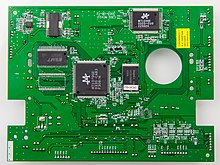
Printed circuit board
Another manufacturing process adds vias, metal-lined drilled holes that enable electrical interconnections between conductive layers, to boards with more than a single side.
In 1903, a German inventor, Albert Hanson, described flat foil conductors laminated to an insulating board, in multiple layers.
The Austrian engineer Paul Eisler invented the printed circuit as part of a radio set while working in the UK around 1936.
Around 1943 the United States began to use the technology on a large scale to make proximity fuzes for use in World War II.
Rubinstein was honored in 1984 by his alma mater, the University of Wisconsin-Madison, for his innovations in the technology of printed electronic circuits and the fabrication of capacitors.
[8][9] This invention also represents a step in the development of integrated circuit technology, as not only wiring but also passive components were fabricated on the ceramic substrate.
Motorola was an early leader in bringing the process into consumer electronics, announcing in August 1952 the adoption of "plated circuits" in home radios after six years of research and a $1M investment.
[12] Even as circuit boards became available, the point-to-point chassis construction method remained in common use in industry (such as TV and hi-fi sets) into at least the late 1960s.
In 1949, Moe Abramson and Stanislaus F. Danko of the United States Army Signal Corps developed the Auto-Sembly process in which component leads were inserted into a copper foil interconnection pattern and dip soldered.
HDI (High Density Interconnect) technology allows for a denser design on the PCB and thus potentially smaller PCBs with more traces and components in a given area.
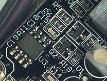
[17] A basic PCB consists of a flat sheet of insulating material and a layer of copper foil, laminated to the substrate.
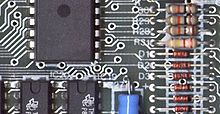
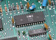
The surface of a PCB may have a coating that protects the copper from corrosion and reduces the chances of solder shorts between traces or undesired electrical contact with stray bare wires.
; each plane of copper is etched, and any internal vias (that will not extend to both outer surfaces of the finished multilayer board) are plated-through, before the layers are laminated together.
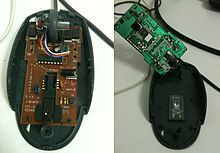
Components were mechanically redesigned to have small metal tabs or end caps that could be soldered directly onto the PCB surface, instead of wire leads to pass through holes.
Surface mounting lends itself well to a high degree of automation, reducing labor costs and greatly increasing production rates compared with through-hole circuit boards.
In a multi-layer board one entire layer may be mostly solid copper to act as a ground plane for shielding and power return.
For microwave circuits, transmission lines can be laid out in a planar form such as stripline or microstrip with carefully controlled dimensions to assure a consistent impedance.
[21] Laminates are manufactured by curing layers of cloth or paper with thermoset resin under pressure and heat to form an integral final piece of uniform thickness.
Thermal expansion is an important consideration especially with ball grid array (BGA) and naked die technologies, and glass fiber offers the best dimensional stability.
The spatially non-homogeneous structure also introduces local variations in electrical parameters, due to different resin/glass ratio at different areas of the weave pattern.
The substrates are characterized by several key parameters, chiefly thermomechanical (glass transition temperature, tensile strength, shear strength, thermal expansion), electrical (dielectric constant, loss tangent, dielectric breakdown voltage, leakage current, tracking resistance...), and others (e.g. moisture absorption).
At the glass transition temperature the resin in the composite softens and significantly increases thermal expansion; exceeding Tg then exerts mechanical overload on the board components - e.g. the joints and the vias.
As the reinforcement and copper confine the board along the plane, virtually all volume expansion projects to the thickness and stresses the plated-through holes.
Choosing unnecessarily low-loss material is a common engineering error in high-frequency digital design; it increases the cost of the boards without a corresponding benefit.
Absorbed moisture can also vaporize on heating, as during soldering, and cause cracking and delamination,[23] the same effect responsible for "popcorning" damage on wet packaging of electronic parts.
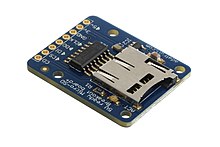
The purpose of a breakout board is to "break out" the leads of a component on separate terminals so that manual connections to them can be made easily.
[32] Multiwire is a patented technique of interconnection which uses machine-routed insulated wires embedded in a non-conducting matrix (often plastic resin).
Before the advent of integrated circuits, this method allowed the highest possible component packing density; because of this, it was used by a number of computer vendors including Control Data Corporation.
This shift is economically efficient from a manufacturer's point of view but is also materially wasteful, as a circuit board with hundreds of functional components may be discarded and replaced due to the failure of one minor and inexpensive part, such as a resistor or capacitor, and this practice is a significant contributor to the problem of e-waste.
[37] In many countries (including all European Single Market participants,[38] the United Kingdom,[39] Turkey, and China), legislation restricts the use of lead, cadmium, and mercury in electrical equipment.