Transistor
Because transistors are the key active components in practically all modern electronics, many people consider them one of the 20th century's greatest inventions.
[2] Physicist Julius Edgar Lilienfeld proposed the concept of a field-effect transistor (FET) in 1925,[3] but it was not possible to construct a working device at that time.
[4] The first working device was a point-contact transistor invented in 1947 by physicists John Bardeen, Walter Brattain, and William Shockley at Bell Labs who shared the 1956 Nobel Prize in Physics for their achievement.
[12] Physicist Julius Edgar Lilienfeld filed a patent for a field-effect transistor (FET) in Canada in 1925,[13] intended as a solid-state replacement for the triode.
Because the production of high-quality semiconductor materials was still decades away, Lilienfeld's solid-state amplifier ideas would not have found practical use in the 1920s and 1930s, even if such a device had been built.
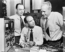
[20] From November 17 to December 23, 1947, John Bardeen and Walter Brattain at AT&T's Bell Labs in Murray Hill, New Jersey, performed experiments and observed that when two gold point contacts were applied to a crystal of germanium, a signal was produced with the output power greater than the input.
[21] Solid State Physics Group leader William Shockley saw the potential in this, and over the next few months worked to greatly expand the knowledge of semiconductors.
[22][23][24] According to Lillian Hoddeson and Vicki Daitch, Shockley proposed that Bell Labs' first patent for a transistor should be based on the field-effect and that he be named as the inventor.
Having unearthed Lilienfeld's patents that went into obscurity years earlier, lawyers at Bell Labs advised against Shockley's proposal because the idea of a field-effect transistor that used an electric field as a "grid" was not new.
[19] To acknowledge this accomplishment, Shockley, Bardeen and Brattain jointly received the 1956 Nobel Prize in Physics "for their researches on semiconductors and their discovery of the transistor effect".
[25][26] Shockley's team initially attempted to build a field-effect transistor (FET) by trying to modulate the conductivity of a semiconductor, but was unsuccessful, mainly due to problems with the surface states, the dangling bond, and the germanium and copper compound materials.
Mataré had previous experience in developing crystal rectifiers from silicon and germanium in the German radar effort during World War II.
On April 12, 1950, Bell Labs chemists Gordon Teal and Morgan Sparks successfully produced a working bipolar NPN junction amplifying germanium transistor.
[34] They were made by etching depressions into an n-type germanium base from both sides with jets of indium(III) sulfate until it was a few ten-thousandths of an inch thick.
4A Toll Crossbar Switching System in 1953, for selecting trunk circuits from routing information encoded on translator cards.
The first prototype pocket transistor radio was shown by INTERMETALL, a company founded by Herbert Mataré in 1952, at the Internationale Funkausstellung Düsseldorf from August 29 to September 6, 1953.
[40][41][42] The first production all-transistor car radio was developed by Chrysler and Philco corporations and was announced in the April 28, 1955, edition of The Wall Street Journal.
[53] In 1948, Bardeen and Brattain patented the progenitor of MOSFET at Bell Labs, an insulated-gate FET (IGFET) with an inversion layer.
[54] In the early years of the semiconductor industry, companies focused on the junction transistor, a relatively bulky device that was difficult to mass-produce, limiting it to several specialized applications.
Field-effect transistors (FETs) were theorized as potential alternatives, but researchers could not get them to work properly, largely due to the surface state barrier that prevented the external electric field from penetrating the material.
Spitzer studied the mechanism of thermally grown oxides, fabricated a high quality Si/SiO2 stack and published their results in 1960.
[79][80] Because transistors are the key active components in practically all modern electronics, many people consider them one of the 20th century's greatest inventions.
[84] Its ability to be mass-produced by a highly automated process (semiconductor device fabrication), from relatively basic materials, allows astonishingly low per-transistor costs.
It is often easier and cheaper to use a standard microcontroller and write a computer program to carry out a control function than to design an equivalent mechanical system.
From mobile phones to televisions, vast numbers of products include amplifiers for sound reproduction, radio transmission, and signal processing.
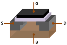
The IGFET is more commonly known as a metal–oxide–semiconductor FET (MOSFET), reflecting its original construction from layers of metal (the gate), oxide (the insulation), and semiconductor.
Functionally, this makes the n-channel JFET the solid-state equivalent of the vacuum tube triode which, similarly, forms a diode between its grid and cathode.
This series sometimes has suffixes, such as R, O, BL, standing for red, orange, blue, etc., to denote variants, such as tighter hFE (gain) groupings.
As older "through-hole" transistors are given surface-mount packaged counterparts, they tend to be assigned many different part numbers because manufacturers have their systems to cope with the variety in pinout arrangements and options for dual or matched n–p–n + p–n–p devices in one pack.
This is included in the table because some silicon power IGFETs have a parasitic reverse Schottky diode formed between the source and drain as part of the fabrication process.