Scanning transmission electron microscopy
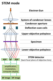
However, unlike CTEM, in STEM the electron beam is focused to a fine spot (with the typical spot size 0.05 – 0.2 nm) which is then scanned over the sample in a raster illumination system constructed so that the sample is illuminated at each point with the beam parallel to the optical axis.
However, at the time the results were inferior to those of transmission electron microscopy, and von Ardenne only spent two years working on the problem.
The microscope was destroyed in an air raid in 1944, and von Ardenne did not return to his work after World War II.
Crewe and coworkers at the University of Chicago developed the cold field emission electron source and built a STEM able to visualize single heavy atoms on thin carbon substrates.
[13] Differential phase contrast (DPC) is an imaging mode which relies on the beam being deflected by electromagnetic fields.
[18] Recently, detectors have been developed for STEM that can record a complete convergent-beam electron diffraction pattern of all scattered and unscattered electrons at every pixel in a scan of the sample in a large four-dimensional dataset (a 2D diffraction pattern recorded at every 2D probe position).
[24] Recently developed monochromators can achieve an energy resolution of ~10 meV in EELS, allowing vibrational spectra to be acquired in STEM.
However, detectors covering large solid angles have been recently developed,[27] and atomic resolution X-ray mapping has even been achieved.
[28] Convergent-beam electron diffraction (CBED) is a STEM technique that provides information about crystal structure at a specific point in a sample.
In CBED, the width of the area a diffraction pattern is acquired from is equal to the size of the probe used, which can be smaller than 1 Å in an aberration-corrected STEM (see above).
[29] Electron microscopy has accelerated research in materials science by quantifying properties and features from nanometer-resolution imaging with STEM, which is crucial in observing and confirming factors, such as thin film deposition, crystal growth, surface structure formation, and dislocation movement.
Until recently, most papers have inferred the properties and behaviors of material systems based on these images without being able to establish rigorous rules for what exactly is observed.
The techniques that have emerged as a result of interest in quantitative scanning transmission electron microscopy (QSTEM) closes this gap by allowing researchers to identify and quantify structural features that are only visible using high-resolution imaging in a STEM.
This ideology has been successfully used to quantify structural properties, such as strain and bond angle, at interfaces and defect complexes.
A notable study is the mapping of atomic column intensities and interatomic bond angles in a mott-insulator system.
[30] This was the first study to show that the transition from the insulating to conducting state was due to a slight global decrease in distortion, which was concluded by mapping the interatomic bond angles as a function of the dopant concentration.
QSTEM analysis can be achieved using commonplace software and programming languages, such as MatLab or Python, with the help of toolboxes and plug-ins that serve to expedite the process.
Universal challenges mainly involve becoming accustomed to the programming language desired and writing software that can tackle the very specific problems for a given material system.
For example, one can imagine how a different analysis technique, and thus a separate image processing algorithm, is necessary for studying ideal cubic versus complex monoclinic structures.
Specialized sample holders or modifications to the microscope can allow a number of additional techniques to be performed in STEM.
[37] Nanoparticles and biological cells have been studied in liquid environments using liquid-phase electron microscopy[38] in STEM, accomplished by mounting a microfluidic enclosure in the specimen holder.
The low energy of the electron beam means that permanent magnets can be used as lenses and thus a miniature column that does not require cooling can be used.