Thermal copper pillar bump
A thermal copper pillar bump, also known as a "thermal bump", is a thermoelectric device made from thin-film thermoelectric material embedded in flip chip interconnects (in particular copper pillar solder bumps) for use in electronics and optoelectronic packaging, including: flip chip packaging of CPU and GPU integrated circuits (chips), laser diodes, and semiconductor optical amplifiers (SOA).
Unlike conventional solder bumps that provide an electrical path and a mechanical connection to the package, thermal bumps act as solid-state heat pumps and add thermal management functionality locally on the surface of a chip or to another electrical component.
Thermal bumps use the thermoelectric effect, which is the direct conversion of temperature differences to electric voltage and vice versa.
The thermal bump pulls heat from one side of the device and transfers it to the other as current is passed through the material.
Thermoelectric power generation (TEG) on the other hand occurs when the thermal bump is subjected to a temperature gradient (i.e., the top is hotter than the bottom).
Nextreme chose the copper pillar bump as an integration strategy due to its widespread acceptance by Intel, Amkor and other industry leaders as the method for connecting microprocessors and other advanced electronics devices to various surfaces during a process referred to as “flip-chip” packaging.
For this reason, the cooling of electronic devices is most efficient when it occurs closest to the source of the heat generation.
The second solution, developed by Delco Electronics (General Motors) in the late 1960s, was similar to embedding copper balls except that the design employed a rigid silver bump.
At the same time, MCNC (which had developed a plated version of IBM’s C4 process) received funding from DARPA to commercialize its technology.
These two organizations, along with APTOS (Advanced Plating Technologies on Silicon), formed the nascent out-sourcing market.
Different solutions were employed including one developed by Focus Interconnect Technology (former APTOS engineers), which used a high aspect ratio plated copper post to provide a larger fixed standoff than was possible for a soft solder collapse joint.
Today, flip chip is a well established technology and collapsed soft solder connections are used in the vast majority of assemblies.
The copper post stand-off developed for the CSP market has found a home in high-density interconnects for advanced micro-processors and is used today by IBM for its CPU packaging.
Trends in high-density interconnects have led to the use of copper pillar solder bumps (CPB) for CPU and GPU packaging.
[2] CPBs are an attractive replacement for traditional solder bumps because they provide a fixed stand-off independent of pitch.
Here the Qmax (maximum heat pumped by a module) is shown to be inversely proportional to the thickness of the film, L.
1 As such, TE coolers manufactured with thin-films can easily have 10x – 20x higher Qmax values for a given active area A.
In addition to the increased heat pumping capability, the use of thin films allows for truly novel implementation of TE devices.
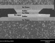
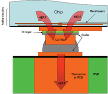
The thermal flow is shown by the arrows labeled “heat.” Metal traces, which can be several micrometres high, can be stacked or interdigitated to provide highly conductive pathways for collecting heat from the underlying circuit and funneling that heat to the thermal bump.
The metal traces shown in the figure for conducting electric current into the thermal bump may or may not be directly connected to the circuitry of the chip.
In this case, the high thermal conductance of the substrate will act as a natural pathway for the rejected heat.
Thermal bumps can be used in a number of different ways to provide chip cooling and power generation.
Because of the small size of the thermal bumps and the relatively high density at which they can be placed on the active surface of the chip, these structures are ideally suited for cooling hotspots.
In addition to chip cooling, thermal bumps can also be applied to high heat-flux interconnects to provide a constant, steady source of power for energy scavenging applications.