X-ray photoelectron spectroscopy
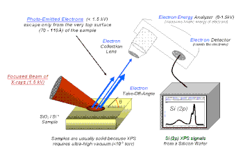
X-ray photoelectron spectroscopy (XPS) is a surface-sensitive quantitative spectroscopic technique that measures the very topmost 200 atoms, 0.01 um, 10 nm of any surface.
It belongs to the family of photoemission spectroscopies in which electron population spectra are obtained by irradiating a material with a beam of X-rays.
It is often applied to study chemical processes in the materials in their as-received state or after cleavage, scraping, exposure to heat, reactive gasses or solutions, ultraviolet light, or during ion implantation.
XPS is routinely used to analyze inorganic compounds, metal alloys, polymers, elements, catalysts, glasses, ceramics, paints, papers, inks, woods, plant parts, make-up, teeth, bones, medical implants, bio-materials,[1] coatings, viscous oils, glues, ion-modified materials and many others.
can be thought of as an adjustable instrumental correction factor that accounts for the few eV of kinetic energy given up by the photoelectron as it gets emitted from the bulk and absorbed by the detector.
Other researchers, including Henry Moseley, Rawlinson and Robinson, independently performed various experiments to sort out the details in the broad bands.
[3] In cooperation with Siegbahn, a small group of engineers (Mike Kelly, Charles Bryson, Lavier Faye, Robert Chaney) at Hewlett-Packard in the US, produced the first commercial monochromatic XPS instrument in 1969.
Siegbahn received the Nobel Prize for Physics in 1981, to acknowledge his extensive efforts to develop XPS into a useful analytical tool.
[4] In parallel with Siegbahn's work, David Turner at Imperial College London (and later at Oxford University) developed ultraviolet photoelectron spectroscopy (UPS) for molecular species using helium lamps.
The number of detected electrons in each peak is directly related to the amount of element within the XPS sampling volume.
To generate atomic percentage values, each raw XPS signal is corrected by dividing the intensity by a relative sensitivity factor (RSF), and normalized over all of the elements detected.
XPS is widely used to generate an empirical formula because it readily yields excellent quantitative accuracy from homogeneous solid-state materials.
Quantitative accuracy depends on several parameters such as: signal-to-noise ratio, peak intensity, accuracy of relative sensitivity factors, correction for electron transmission function, surface volume homogeneity, correction for energy dependence of electron mean free path, and degree of sample degradation due to analysis.
Detection limits may vary greatly with the cross section of the core state of interest and the background signal level.
This level of heat, when combined with the Bremsstrahlung X-rays, acts to increase the amount and rate of degradation for certain materials.
[citation needed] Typically ranging 1–20 minutes for a broad survey scan that measures the amount of all detectable elements, typically 1–15 minutes for high resolution scan that reveal chemical state differences (for a high signal/noise ratio for count area result often requires multiple sweeps of the region of interest), 1–4 hours for a depth profile that measures 4–5 elements as a function of etched depth (this process time can vary the most as many factors will play a role).
The ability to produce chemical state information, i.e. the local bonding environment of an atomic species in question from the topmost few nanometers of the sample makes XPS a unique and valuable tool for understanding the chemistry of the surface.
Sometimes, however, much simpler electron energy filters - the cylindrical mirror analyzers are used, most often for checking the elemental composition of the surface.
Under practical conditions, high energy-resolution settings produce peak widths (FWHM) between 0.4 and 0.6 eV for various elements and some compounds.
[citation needed] Non-monochromatic magnesium X-rays have a wavelength of 9.89 angstroms (0.989 nm) which corresponds to a photon energy of 1253 eV.
The ultimate energy resolution (FWHM) when using a non-monochromatic Mg Kα source is 0.9–1.0 eV, which includes some contribution from spectrometer-induced broadening.
[citation needed] A breakthrough has been brought about in the last decades by the development of large scale synchrotron radiation facilities.
The Hippie beam line of this facility also allows to perform in operando Ambient Pressure X-Ray Photoelectron Spectroscopy (AP-XPS9.
Tables of binding energies that identify the shell and spin-orbit of each peak produced by a given element are included with modern XPS instruments, and can be found in various handbooks and websites.
Before beginning the process of peak identification, the analyst must determine if the binding energies of the unprocessed survey spectrum (0-1400 eV) have or have not been shifted due to a positive or negative surface charge.
The process of peak-fitting high energy resolution XPS spectra is a mixture of scientific knowledge and experience.
If the top 15 nm is a homogeneous material with only very minor amounts of adventitious carbon and adsorbed gases, then the analyst can use theoretical peak area ratios to enhance the peak-fitting process.
From the theoretical point of view, the photoemission process from a solid can be described with a semiclassical approach, where the electromagnetic field is still treated classically, while a quantum-mechanical description is used for matter.
The first effect is caused by the non perfect monochromaticity of the photon beam -which results in a finite bandwidth- and by the limited resolving power of the analyzer.
Temperature-dependent atomic lattice vibrations, or phonons, can broaden the core level components and attenuate the interference patterns in an X-ray photoelectron diffraction (XPD) experiment.