Cache hierarchy
[4] CPUs were increasingly capable of running and executing larger amounts of instructions in a given time, but the time needed to access data from main memory prevented programs from fully benefiting from this capability.
[5] This issue motivated the creation of memory models with higher access rates in order to realize the potential of faster processors.
[6] This resulted in the concept of cache memory, first proposed by Maurice Wilkes, a British computer scientist at the University of Cambridge in 1965.
[7] Between roughly 1970 and 1990, papers and articles by Anant Agarwal, Alan Jay Smith, Mark D. Hill, Thomas R. Puzak, and others discussed better cache memory designs.
This need resulted from the fact that although early cache models improved data access latency, with respect to cost and technical limitations it was not feasible for a computer system's cache to approach the size of main memory.
Jean-Loup Baer, Wen-Hann Wang, Andrew W. Wilson, and others have conducted research on this model.
[8] Accessing main memory for each instruction execution may result in slow processing, with the clock speed depending on the time required to find and fetch the data.
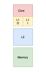
[10] This structure resides closer to the processor in terms of the time taken to search and fetch data with respect to the main memory.
[13] In the case of a cache miss, the purpose of using such a structure will be rendered useless and the computer will have to go to the main memory to fetch the required data.
The general trend is to keep the L1 cache small and at a distance of 1–2 CPU clock cycles from the processor, with the lower levels of caches increasing in size to store more data than L1, hence being more distant but with a lower miss rate.
[15] The number of cache levels can be designed by architects according to their requirements after checking for trade-offs between cost, AATs, and size.
[16][17] With the technology-scaling that allowed memory systems able to be accommodated on a single chip, most modern day processors have up to three or four cache levels.
Having multiple ports requires additional hardware and wiring, leading to a significant structure between the caches and processing units.
[citation needed] In the case of write through policy, whenever the value of the cache block changes, it is further modified in the lower-level memory hierarchy as well.
Under this policy, there is a risk for data-loss as the most recently changed copy of a datum is only stored in the cache and therefore some corrective techniques must be observed.
However, this type of design choice in a multi-layer cache architecture can also be good for a lower data-access latency.