Carbon nanotube field-effect transistor
[1][2] According to Moore's law, the dimensions of individual devices in an integrated circuit have been decreased by a factor of approximately two every two years.
However, as noted by ITRS 2009 edition, further scaling down has faced serious limits related to fabrication technology and device performances as the critical dimension shrunk down to sub-22 nm range.
[5] Because of the strong covalent carbon–carbon bonding in the sp2 configuration, carbon nanotubes are chemically inert and are able to transport large electric currents.
In theory, carbon nanotubes are also able to conduct heat nearly as well as diamond or sapphire, and because of their miniaturized dimensions, the CNTFET should switch reliably using much less power than a silicon-based device.
[6] To a first approximation, the exceptional electrical properties of carbon nanotubes can be viewed as inherited from the unique electronic structure of graphene, provided the carbon nanotube is thought of as graphene rolled up along one of its Bravais lattice vectors Ĉh to form a hollow cylinder.
[7] [8] [9] In this construction, periodic boundary conditions are imposed over Ĉh to yield a lattice of seamlessly bonded carbon atoms on the cylinder surface.
[10] Thus, the circumference of such a carbon nanotube can be expressed in terms of its rollup vector: Ĉh=nâ1+mâ2 that connects two crystallographically equivalent sites of the two-dimensional graphene sheet.
These results can be motivated by noting that periodic boundary conditions for 1D carbon nanotubes permit only a few wave vectors to exist around their circumferences.
The earliest techniques for fabricating carbon nanotube (CNT) field-effect transistors involved pre-patterning parallel strips of metal across a silicon dioxide substrate, and then depositing the CNTs on top in a random pattern.
[1][2] The semiconducting CNTs that happened to fall across two metal strips meet all the requirements necessary for a rudimentary field-effect transistor.
Also, due to the semiconducting nature of the CNT, a Schottky barrier forms at the metal–semiconductor interface,[17] increasing the contact resistance.
Its thickness made it difficult to switch the devices on and off using low voltages, and the fabrication process led to poor contact between the gate dielectric and CNT.
After an individual tube is isolated, source and drain contacts are defined and patterned using high resolution electron beam lithography.
Arrays of top-gated CNTFETs can be fabricated on the same wafer, since the gate contacts are electrically isolated from each other, unlike in the back-gated case.
These advantages mean top-gated devices are generally preferred over back-gated CNTFETs, despite their more complex fabrication process.
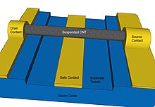
Yet another CNTFET device geometry involves suspending the nanotube over a trench to reduce contact with the substrate and gate oxide.
This technique will also only work for shorter nanotubes, as longer tubes will flex in the middle and droop towards the gate, possibly touching the metal contact and shorting the device.
In general, suspended CNTFETs are not practical for commercial applications, but they can be useful for studying the intrinsic properties of clean nanotubes.
For planar CNTFETs with different design parameters, the FET with a shorter channel length produces a higher saturation current, and the saturation drain current also becomes higher for the FET consisting of smaller diameter keeping the length constant.
[30] When an electric field is applied to a CNT transistor, a mobile charge is induced in the tube from the source and drain.
The decrease of the current and burning of the CNT can occur due to the temperature raised by several hundreds of kelvins.
Generally, the self-heating effect is much less severe in a semiconducting CNTFET than in a metallic one due to different heat dissipation mechanisms.
[citation needed] The first sub-10-nanometer CNT transistor was made which outperformed the best competing silicon devices with more than four times the diameter-normalized current density (2.41 mA/μm) at an operating voltage of 0.5 V. The inverse subthreshold slope of the CNTFET was 94 mV/decade.
[34] Carbon nanotubes have shown reliability issues when operated under high electric field or temperature gradients.
Applying high voltages beyond avalanche point results in Joule heating and eventual breakdown in CNTs.
To overcome the fabrication difficulties, several methods have been studied such as direct growth, solution dropping, and various transfer printing techniques.
[37] The most promising methods for mass production involve some degree of self-assembly of pre-produced nanotubes into the desired positions.
Individually manipulating many tubes is impractical at a large scale and growing them in their final positions presents many challenges.
The most desirable future work involved in CNTFETs will be the transistor with higher reliability, cheap production cost, or the one with more enhanced performances.
For example: adding effects external to the inner CNT transistor like the Schottky barrier between the CNT and metal contacts, multiple CNTs at a single gate,[30] channel fringe capacitances, parasitic source/drain resistance, and series resistance due to the scattering effects.