Dip-pen nanolithography
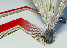
Dip pen nanolithography (DPN) is a scanning probe lithography technique where an atomic force microscope (AFM) tip is used to directly create patterns on a substrate.
A research group at Northwestern University, US led by Chad Mirkin independently studied the process and determined that under the appropriate conditions, molecules could be transferred to a wide variety of surfaces to create stable chemically-adsorbed monolayers in a high resolution lithographic process they termed "DPN".
[6] Mirkin and his coworkers hold the patents on this process,[7] and the patterning technique has expanded to include liquid "inks".
Molecular inks are typically composed of small molecules that are coated onto a DPN tip and are delivered to the surface through a water meniscus.
Direct-write techniques, like contact printing, can pattern multiple biological materials but it cannot create features with subcellular resolution.
Many high-resolution lithography methods can pattern at sub-micrometre resolution, but these require high-cost equipment that were not designed for biomolecule deposition and cell culture.
The particles are suspended in a Poly(methyl methacrylate) (PMMA) or equivalent polymer matrix, and heated by the probe tip until they begin to flow.
An O2 plasma etch can be used to remove the PMMA matrix, and in the case of Iron Oxide nanoparticles, further reduce the resolution of lines to 10 nm.
[22] Advantages unique to tDPL are that it is a maskless additive process that can achieve very narrow resolutions, it can also easily write many types of nanoparticles without requiring special solution preparation techniques.
[22] A two dimensional array of (PDMS) deformable transparent pyramid shaped tips are coated with an opaque layer of metal.
DPN is a maskless direct write technique that can be used to create multiple patterns of varying size, shape, and feature resolution, all on a single substrate.
No one would try to apply microcontact printing to such a project because then it would never be worth the time and money required to fabricate each master stamp for each new pattern.
With virtually all ink/substrate combinations, the same feature size will be patterned no matter how hard the tip is pressing down against the surface.