Scanning SQUID microscopy
The first scanning SQUID microscope was built in 1992 by Black et al.[2] Since then the technique has been used to confirm unconventional superconductivity in several high-temperature superconductors including YBCO and BSCCO compounds.
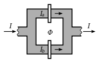
A DC SQUID consists of superconducting electrodes in a ring pattern connected by two weak-link Josephson junctions (see figure).
However, as noted by the figure, the voltage across the electrodes oscillates sinusoidally with respect to the amount of magnetic flux passing through the device.
Most common is a shield made of mu-metal, possibly in combination with a superconducting "can" (all superconductors repel magnetic fields via the Meissner effect).
Operating at lower-tip sample distances increases the sensitivity and resolution of the device, but requires more advanced mechanisms in controlling the height of the probe.
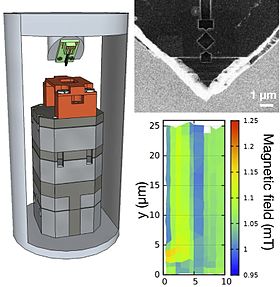
The microscope uses a patented design to allow the sample under investigation to be at room temperature and in air while the SQUID sensor is under vacuum and cooled to less than 80 K using a cryo cooler.
The system's output is displayed as a false-color image of magnetic field strength or current magnitude (after processing) versus position on the sample.
[6] Operation of a scanning SQUID microscope consists of simply cooling down the probe and sample, and rastering the tip across the area where measurements are desired.
The scanning SQUID microscope was originally developed for an experiment to test the pairing symmetry of the high-temperature cuprate superconductor YBCO.
In YBCO, upon crossing the [110] planes in momentum (and real) space, the wavefunction will undergo a phase shift of π.
Hence if one forms a Josephson ring device where this plane is crossed (2n+1), number of times, a phase difference of (2n+1)π will be observed between the two junctions.
In the same property behind the scanning SQUID microscope, the phase of the wavefunction is also altered by the amount of magnetic flux passing through the junction, following the relationship Δφ=π(Φ0).
The device observed zero field at B, C, and D. The results provided one of the earliest and most direct experimental confirmations of d-wave pairing in YBCO.
SQUID scanning can also isolate defective components in assembled devices or Printed Circuit Board (PCB).
To date, Scanning Acoustic Microscopy (SAM), Time Domain Reflectometry (TDR) analysis, and Real-Time X-ray (RTX) inspection were the non-destructive tools used to detect short faults.
Because of the high density wire bonding in advanced wire-bond packages, it is extremely hard to localize the short with conventional RTX inspection.
Without detailed information as to where the short might occur, attempting destructive decapsulation to expose both die surface and bond wires is full of risk.
Based on the data analysis, fault localization by SSM should isolate the short in the die, bond wires or package substrate.
For instance, when an electric short is produced by two bond wires touching each other, X-ray analysis may help to identify potential defect locations; however, defects like metal migration produced at wirebond pads, or bond wires somehow touching any other conductive structures, may be very difficult to catch with non-destructive techniques that are not electrical in nature.
Here, the availability of analytical tools that can map out the flow of electric current inside the package provide valuable information to guide the failure analyst to potential defect locations.
The X-ray image of figure 1b is intended to illustrate the challenge of finding the potential short locations represented for failure analysts.
After obtaining similar SSM results on the two units under test, further destructive analysis focused around the small potential short region, and it showed that the failing pin wirebond is touching the bottom of one of the stacked dice at the specific XY position highlighted by SSM analysis.
We used the SQUID facilities at Neocera to investigate the failure in the package of interest, with pins carrying 1.47 milliamps at 2 volts.
The second fault location technique will be taken somewhat out of turn, as it was used to characterize this failure after the SQUID analysis, as an evaluation sample for an equipment vendor.
The feature shown (which is also the material responsible for the failure) is a copper filament approximately three micrometres wide in cross-section, which was impossible to resolve in our in-house radiography equipment.
The principal drawback of this technique is that the depth of field is extremely short, requiring many ‘cuts’ on a given specimen to detect very small particles or filaments.
At the high magnification required to resolve micrometre-sized features, the technique can become prohibitively expensive in both time and money to perform.
Similarly electrical overstress was considered an unlikely cause of failure as the part had not been under power since the time it was qualified at the factory.
As for all near field situations, the resolution is limited by the scanning distance or, ultimately, by the sensor size (typical SQUIDs are about 30 μm wide), although software and data acquisition improvements allow locating currents within 3 micrometres.
This does not mean that we are missing vertical information; in the simplest situation, if a current path jumps from one plane to another, getting closer to the sensor in the process, this will be revealed as stronger magnetic field intensity for the section closer to the sensor and also as higher intensity in the current density map.