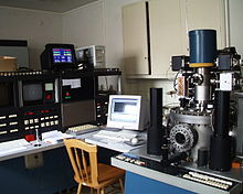
Electron-beam lithography
The purpose, as with photolithography, is to create very small structures in the resist that can subsequently be transferred to the substrate material, often by etching.
The primary advantage of electron-beam lithography is that it can draw custom patterns (direct-write) with sub-10 nm resolution.
This form of maskless lithography has high resolution but low throughput, limiting its usage to photomask fabrication, low-volume production of semiconductor devices, and research and development.
Newer systems use shaped beams that can be deflected to various positions in the writing field (also known as vector scan).
However, systems with higher-resolution requirements need to use field electron emission sources, such as heated W/ZrO2 for lower energy spread and enhanced brightness.
Because of the inaccuracy and because of the finite number of steps in the exposure grid, the writing field is of the order of 100 micrometre – 1 mm.
For example, assuming an exposure area of 1 cm2, a dose of 10−3 coulombs/cm2, and a beam current of 10−9 amperes, the resulting minimum write time would be 106 seconds (about 12 days).
To cover the 700 cm2 surface area of a 300 mm silicon wafer, the minimum write time would extend to 7*108 seconds, about 22 years.
It is clear that throughput is a serious limitation for electron beam lithography, especially when writing dense patterns over a large area.
The smaller field of electron beam writing makes for very slow pattern generation compared with photolithography (the current standard) because more exposure fields must be scanned to form the final pattern area (≤mm2 for electron beam vs. ≥40 mm2 for an optical mask projection scanner).
As soon as the number reaches ~10000, shot noise effects become predominant, leading to substantial natural dose variation within a large feature population.
With each successive process node, as the feature area is halved, the minimum dose must double to maintain the same noise level.
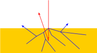
These secondary electrons are capable of breaking bonds (with binding energy E0) at some distance away from the original collision.
[12] On the other hand, it is already known that the mean free path at the lowest energies (few to several eV or less, where dissociative attachment is significant) is well over 10 nm,[13][14] thus limiting the ability to consistently achieve resolution at this scale.
[15][16] This point was driven home by a 2007 demonstration of double patterning using electron beam lithography in the fabrication of 15 nm half-pitch zone plates.
The use of double patterning allowed the spacing between features to be wide enough for the secondary electron scattering to be significantly reduced.
It is now recognized that for insulating materials like PMMA, low energy electrons can travel quite a far distance (several nm is possible).
[19] The travel distance of secondary electrons is not a fundamentally derived physical value, but a statistical parameter often determined from many experiments or Monte Carlo simulations down to < 1 eV.
[15] Repeatability and control at the practical resolution limit often require considerations not related to image formation, e.g., resist development and intermolecular forces.
For thicker resists, as the primary electrons move forward, they have an increasing opportunity to scatter laterally from the beam-defined location.
A large enough dose of backscattered electrons can lead to complete exposure of resist over an area much larger than defined by the beam spot.
[28] The proximity effect is also manifest by secondary electrons leaving the top surface of the resist and then returning some tens of nanometers distance away.
[29] Proximity effects (due to electron scattering) can be addressed by solving the inverse problem and calculating the exposure function E(x,y) that leads to a dose distribution as close as possible to the desired dose D(x,y) when convolved by the scattering distribution point spread function PSF(x,y).
However, it must be remembered that an error in the applied dose (e.g., from shot noise) would cause the proximity effect correction to fail.
Due to the scission efficiency generally being an order of magnitude higher than the crosslinking efficiency, most polymers used for positive-tone electron-beam lithography will also crosslink (and therefore become negative tone) at doses an order of magnitude higher than the doses used to cause scission in the polymer for positive tone exposure.
[31][32][33] A study performed at the Naval Research Laboratory[34] indicated that low-energy (10–50 eV) electrons were able to damage ~30 nm thick PMMA films.
[39] The data suggest that electrons with energies as low as 12 eV can penetrate 50 nm thick polymer resist.
Another alternative in electron-beam lithography is to use extremely high electron energies (at least 100 keV) to essentially "drill" or sputter the material.
As a result, it is a slow process, requiring much longer exposure times than conventional electron beam lithography.
There has been significant interest in the development of multiple electron beam approaches to lithography in order to increase throughput.