Embedded wafer level ball grid array
Embedded wafer level ball grid array (eWLB) is a packaging technology for integrated circuits.
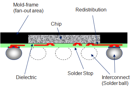
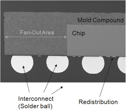
It is common for all WLB technologies, which are built on a silicon wafer, that the interconnects (typically solder balls) fit on the chip (so called fan-in design).
After curing an artificial wafer containing a mold frame around the dies for carrying additional interconnect elements is created.
Therefore, this wafer level packaging technology can also be used for space sensitive applications, where the chip area wouldn’t be sufficient to place the required number of interconnects at a suitable distance.
The eWLB technology was developed by Infineon, STMicroelectronics and STATS ChipPAC Ltd.[1] First components were brought into market mid of 2009 (mobile phone).