Hybrid integrated circuit
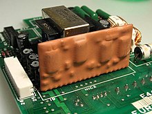
Hybrid circuits could be encapsulated in epoxy, as shown in the photo, or in military and space applications, a lid was soldered onto the package.
[3] In military and space applications, numerous integrated circuits, transistors and diodes, in their die form, would be placed on either a ceramic or beryllium substrate.
Multi-layer thick film is a technique for further improvements in integration using a screen printed insulating dielectric to ensure connections between layers are made only where required.
One key advantage for the circuit designer is complete freedom in the choice of resistor value in thick film technology.
Once the hybrid circuit is fully populated with components, fine tuning prior to final test may be achieved by active laser trimming.
Capacitors and semiconductors were in the form of LID (Leadless Inverted Devices) soldered to the surface by selectively heating the substrate from the underside.