MOSFET
Similarly, "oxide" in the name can also be a misnomer, as different dielectric materials are used with the aim of obtaining strong channels with smaller applied voltages.
As MOSFETs can be made with either p-type or n-type semiconductors, complementary pairs of MOS transistors can be used to make switching circuits with very low power consumption, in the form of CMOS logic.
[3] In the 1940s, Bell Labs scientists William Shockley, John Bardeen and Walter Houser Brattain attempted to build a field-effect device, which led to their discovery of the transistor effect.
[citation needed] Many semiconductors with better electrical properties than silicon, such as gallium arsenide, do not form good semiconductor-to-insulator interfaces, and thus are not suitable for MOSFETs.
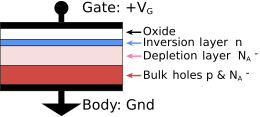
When a voltage is applied between the gate and the source, the electric field generated penetrates through the oxide and creates an inversion layer or channel at the semiconductor-insulator interface.
Varying the voltage between the gate and body modulates the conductivity of this layer and thereby controls the current flow between drain and source.
If we consider a p-type semiconductor (with NA the density of acceptors, p the density of holes; p = NA in neutral bulk), a positive voltage, VG, from gate to body (see figure) creates a depletion layer by forcing the positively charged holes away from the gate-insulator/semiconductor interface, leaving exposed a carrier-free region of immobile, negatively charged acceptor ions (see doping).
As the voltage at the gate increases, there will be a point at which the surface above the depletion region will be converted from p-type into n-type, as electrons from the bulk area will start to get attracted by the larger electric field.
For gate voltages below the threshold value, the channel is lightly populated, and only a very small subthreshold leakage current can flow between the source and the drain.
is the body effect parameter, and 2φB is the approximate potential drop between surface and bulk across the depletion layer when VSB = 0 and gate bias is sufficient to ensure that a channel is present.
Analog circuits depend on operation in the transition region where small changes to Vgs can modulate the output (drain) current.
Nevertheless, MOSFETs are widely used in many types of analog circuits because of their own advantages (zero gate current, high and adjustable output impedance and improved robustness vs. BJTs which can be permanently degraded by even lightly breaking down the emitter-base).
[dubious – discuss] This means that complete analog circuits can be made on a silicon chip in a much smaller space and with simpler fabrication techniques.
Some ICs combine analog and digital MOSFET circuitry on a single mixed-signal integrated circuit, making the needed board space even smaller.
Highly doped polycrystalline silicon is an acceptable but certainly not ideal conductor, and also suffers from some more technical deficiencies in its role as the standard gate material.
The drain induced barrier lowering of the threshold voltage and channel length modulation effects upon I-V curves are reduced by using shallow junction extensions.
[55] The capacitive effects are limited by using raised source and drain geometries that make most of the contact area border thick dielectric instead of silicon.
While this has been traditionally the case for the older technologies, for the state-of-the-art MOSFETs reduction of the transistor dimensions does not necessarily translate to higher chip speed because the delay due to interconnections is more significant.
Producing MOSFETs with channel lengths much smaller than a micrometre is a challenge, and the difficulties of semiconductor device fabrication are always a limiting factor in advancing integrated circuit technology.
The maximum gate-source voltage is determined by the strength of the electric field able to be sustained by the gate dielectric before significant leakage occurs.
Heavier doping is also associated with thinner depletion layers and more recombination centers that result in increased leakage current, even without lattice damage.
The transconductance of the MOSFET decides its gain and is proportional to hole or electron mobility (depending on device type), at least for low drain voltages.
In addition, microscopic variations in structure due simply to the probabilistic nature of atomic processes require statistical (not just deterministic) predictions.
It is commonly used for small-signal devices in radio frequency applications where biasing the drain-side gate at constant potential reduces the gain loss caused by Miller effect, replacing two separate transistors in cascode configuration.
Vacuum-tube tetrodes, using a screen grid, exhibit much lower grid-plate capacitance and much higher output impedance and voltage gains than triode vacuum tubes.
The FinFET is a double-gate silicon-on-insulator device, one of a number of geometries being introduced to mitigate the effects of short channels and reduce drain-induced barrier lowering.
Depletion-mode MOSFET families include the BF960 by Siemens and Telefunken, and the BF980 in the 1980s by Philips (later to become NXP Semiconductors), whose derivatives are still used in AGC and RF mixer front-ends.
Semiconductor sub-micrometer and nanometer electronic circuits are the primary concern for operating within the normal tolerance in harsh radiation environments like outer space.
The ELT offers many advantages, including an improvement of reliability by reducing unwanted surface inversion at the gate edges which occurs in the standard MOSFET.
Low-power microelectronic circuits including computers, communication devices, and monitoring systems in space shuttles and satellites are very different from what is used on earth.