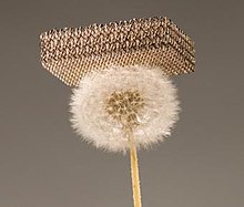
Metallic microlattice
[1] It was developed by a team of scientists from California-based HRL Laboratories, in collaboration with researchers at University of California, Irvine and Caltech, and was first announced in November 2011.
[4] A detailed comparative review study among other types of metallic lattice structures showed them to be beneficial for light-weighting purposes but expensive to manufacture.
The process was similar to photolithography in that it used a two-dimensional mask to define the starting template structure, but differed in the rate of formation: where stereolithography might take hours to make a full structure, the self-forming waveguide process allowed templates to be formed in 10–100 seconds.
Their Young's modulus E exhibits different scaling, with the density ρ, E ~ ρ2, compared to E ~ ρ3 in aerogels and carbon nanotube foams.
[8] Metallic microlattice may find potential applications in thermal and vibration insulators such as shock absorbers, and may also prove useful as battery electrodes and catalyst supports.
[8] Additionally, the microlattices' ability to return to their original state after being compressed may make them suitable for use in spring-like energy storage devices.
[4] A similar but denser material, consisting of an electrodeposited nanocrystalline nickel layer over a polymeric rapid-prototyped truss, was created by researchers at the University of Toronto in 2008.