Flip-flop (electronics)
The term flip-flop has historically referred generically to both level-triggered (asynchronous, transparent, or opaque) and edge-triggered (synchronous, or clocked) circuits that store a single bit of data using gates.
[1] Modern authors reserve the term flip-flop exclusively for edge-triggered storage elements and latches for level-triggered ones.
[4] When a level-triggered latch is enabled it becomes transparent, but an edge-triggered flip-flop's output only changes on a clock edge (either positive going or negative going).
According to P. L. Lindley, an engineer at the US Jet Propulsion Laboratory, the flip-flop types detailed below (SR, D, T, JK) were first discussed in a 1954 UCLA course on computer design by Montgomery Phister, and then appeared in his book Logical Design of Digital Computers.
[11][12] Lindley was at the time working at Hughes Aircraft under Eldred Nelson, who had coined the term JK for a flip-flop which changed states when both inputs were on (a logical "one").
Lindley explains that he heard the story of the JK flip-flop from Eldred Nelson, who is responsible for coining the term while working at Hughes Aircraft.
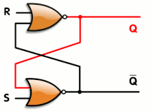
Thus the two stages are connected in a non-inverting loop although the circuit diagram is usually drawn as a symmetric cross-coupled pair (both the drawings are initially introduced in the Eccles–Jordan patent).
Flip-flops and latches can be divided into common types: SR ("set-reset"), D ("data"), T ("toggle"), and JK (see History section above).
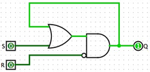
The SR NOR latch consists of two parallel NOR gates where the output of each NOR is also fanned out into one input of the other NOR, as shown in the figure.
The output could remain in a metastable state and may eventually lock at either 1 or 0 depending on the propagation time relations between the gates (a race condition).
From a teaching point of view, SR latches drawn as a pair of cross-coupled components (transistors, gates, tubes, etc.)
A didactically easier explanation is to draw the latch as a single feedback loop instead of the cross-coupling.
The SR AND-OR latch is easier to understand, because both gates can be explained in isolation, again with the control view of AND and OR from above.
With E low (enable false) the latch is closed (opaque) and remains in the state it was left the last time E was high.
[18] The merge is commonly exploited in the design of pipelined computers, and, in fact, was originally developed by John G. Earle to be used in the IBM System/360 Model 91 for that purpose.
[21] If the middle NAND gate is omitted, then one gets the polarity hold latch, which is commonly used because it demands less logic.
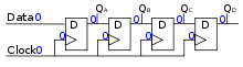
Here is the truth table for the other possible S and R configurations: These flip-flops are very useful, as they form the basis for shift registers, which are an essential part of many electronic devices.
This allows the "master" latch to store the input value when the clock signal transitions from low to high.
Nearly simultaneously, the twice inverted "enable" of the second or "slave" D latch transitions from low to high (0 to 1) with the clock signal.
Removing the leftmost inverter in the circuit creates a D-type flip-flop that strobes on the falling edge of a clock signal.
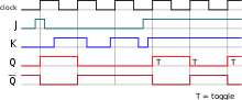
The characteristic equation of the JK flip-flop is: and the corresponding truth table is: The input must be held steady in a period around the rising edge of the clock known as the aperture.
The differentiation offers circuit designers the ability to define the verification conditions for these types of signals independently.
Depending upon the flip-flop's internal organization, it is possible to build a device with a zero (or even negative) setup or hold time requirement but not both simultaneously.
Unfortunately, it is not always possible to meet the setup and hold criteria, because the flip-flop may be connected to a real-time signal that could change at any time, outside the control of the designer.
In this case, the best the designer can do is to reduce the probability of error to a certain level, depending on the required reliability of the circuit.
One technique for suppressing metastability is to connect two or more flip-flops in a chain, so that the output of each one feeds the data input of the next, and all devices share a common clock.
So-called metastable-hardened flip-flops are available, which work by reducing the setup and hold times as much as possible, but even these cannot eliminate the problem entirely.
When the transitions in the clock and the data are close together in time, the flip-flop is forced to decide which event happened first.
In this case, dual-ranked flip-flops that are clocked slower than the maximum allowed metastability time will provide proper conditioning for asynchronous (e.g., external) signals.
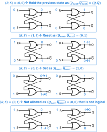
In this case the memory element retains exactly one of the logic states until the control inputs induce a change.


- S = 1, R = 0: Set
- S = 0, R = 0: Hold
- S = 0, R = 1: Reset
- S = 1, R = 1: Not allowed