Selected area diffraction
It is a specific case of electron diffraction used primarily in material science and solid state physics as one of the most common experimental techniques.
Especially with appropriate analytical software, SAD patterns (SADP) can be used to determine crystal orientation, measure lattice constants or examine its defects.
Due to the wave–particle duality, the high-energetic electrons behave as matter waves with wavelength of a few thousandths of a nanometer.
Due to the constructive interference, the spherical waves from number of diffracted beams under angles
After being deflected by the microscope's magnetic lens, each set of initially parallel beams intersect in the back focal plane forming the diffraction pattern.
This allows to study small objects such as crystallites in polycrystalline material with a broad parallel beam.
For two reasons, these conditions result in a diffractogram of concentric rings: SAD analysis is widely used in material research for its relative simplicity and high information value.
Once the sample is prepared and examined in a modern transmission electron microscope, the device allows for a routine diffraction acquisition in a matter of seconds.
The course of analysis depends on whether the diffractogram depicts ring or spot diffraction pattern and on the quantity to be determined.
Software tools based on computer vision algorithms simplifies quantitative analysis.
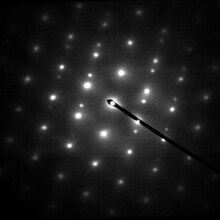
[4] If the SAD is taken from one a or a few single crystals, the diffractogram depicts a regular pattern of bright spots.
Even though the SAD-based analyses were not considered quantitative for a long time, computer tools brought accuracy and repeatability allowing to routinely perform accurate measurements of interplanar distances or angles on appropriately calibrated microscopes.
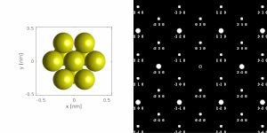
A series of diffractograms varying in tilt can be acquired and processed with diffraction tomography analysis in order to reconstruct an unknown crystal structure.
If the illuminated area selected by the aperture covers many differently oriented crystallites, their diffraction patterns superimpose forming an image of concentric rings.
Diameter of each ring corresponds to interplanar distance of a plane system present in the sample.
The transmitted beam is often too strong and needs to be shadowed with a beam-stopper in order to protect the camera.
Then, they can be processed the same way as real diffractograms allowing to determine crystal orientation, measure interplanar angles and distances even with picometric precision.