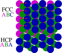
Stacking fault
Stacking faults are two dimensional planar defects that can occur in crystalline materials.
[4] Splitting into two partial dislocations is favorable because the energy of a line defect is proportional to the square of the burger’s vector magnitude.
The force of repulsion depends on factors such as shear modulus, burger’s vector, Poisson’s ratio, and distance between the dislocations.
By nature of stacking fault being a defect, it has higher energy than that of a perfect crystal, so acts to attract the partial dislocations together again.
Stacking faults may also be created by Frank partial dislocations with burger’s vector of 1/3<111>.
[4] There are two types of stacking faults caused by Frank partial dislocations: intrinsic and extrinsic.
[5] An extrinsic stacking fault is formed from interstitial agglomeration, where there is an extra plane with sequence ABCA_BAC_ABCA.
In order to identify the stacking fault, it is important to recognize the exact Bragg condition for certain lattice planes in the matrix such that regions without defects will detect little backscattered electrons and thus appear dark.
Meanwhile, regions with the stacking fault will not satisfy the Bragg condition and thus yield high amounts of backscattered electrons, and thus appear bright in the image.
Inverting the contrast gives images where the stacking fault appears dark in the midst of a bright matrix.
[7] In a TEM, bright field imaging is one technique used to identify the location of stacking faults.
In a semiconductor crystal, the fcc and hcp phases of a given material will usually have different band gap energies.
As a consequence, when the crystal phase of a stacking fault has a lower band gap than the surrounding phase, it forms a quantum well, which in photoluminescence experiments leads to light emission at lower energies (longer wavelengths) than for the bulk crystal.