Operational amplifier applications
Operational amplifiers are optimised for use with negative feedback, and this article discusses only negative-feedback applications.
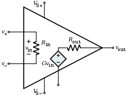
In this article, a simplified schematic notation is used that ignores details such as device selection and power supply connections.
The operational amplifier must With these requirements satisfied, one can use the method of virtual ground to quickly and intuitively grasp the behavior of the op-amp circuits.
Resistors much greater than 1 MΩ cause excessive thermal noise and make the circuit operation susceptible to significant errors due to bias or leakage currents.
Appropriate design of the feedback network can alleviate problems associated with input bias currents and common-mode gain, as explained below.
Alternatively, a tunable external voltage can be added to one of the inputs in order to balance out the offset effect.
In cases where a design calls for one input to be short-circuited to ground, that short circuit can be replaced with a variable resistance that can be tuned to mitigate the offset problem.
This problem can be mitigated with appropriate use of bypass capacitors connected across each power supply pin and ground.
The output voltage Or, expressed as a function of the common-mode input Vcom and difference input Vdif: the output voltage is In order for this circuit to produce a signal proportional to the voltage difference of the input terminals, the coefficient of the Vcom term (the common-mode gain) must be zero, or With this constraint[nb 1] in place, the common-mode rejection ratio of this circuit is infinitely large, and the output where the simple expression Rf / R1 represents the closed-loop gain of the differential amplifier.
The closed-loop gain is Rf / Rin, hence The simplified circuit above is like the differential amplifier in the limit of R2 and Rg very small.
In this case, though, the circuit will be susceptible to input bias current drift because of the mismatch between Rf and Rin.
When Vin descends "below ground", the output Vout rises proportionately to balance the seesaw, and vice versa.
Referring to the circuit immediately above, To intuitively see this gain equation, use the virtual ground technique to calculate the current in resistor R1: then recall that this same current must be passing through R2, therefore: Unlike the inverting amplifier, a non-inverting amplifier cannot have a gain of less than 1.
In these cases, a lag compensation network (e.g., connecting the load to the voltage follower through a resistor) can be used to restore stability.
The manufacturer data sheet for the operational amplifier may provide guidance for the selection of components in external compensation networks.
Operational amplifiers can be used in construction of active filters, providing high-pass, low-pass, band-pass, reject and delay functions.
The high input impedance and gain of an op-amp allow straightforward calculation of element values, allowing accurate implementation of any desired filter topology with little concern for the loading effects of stages in the filter or of subsequent stages.
However, it is usually better to use a dedicated comparator for this purpose, as its output has a higher slew rate and can reach either power supply rail.
This can be due to any combination of: The following slightly more complex circuit can ameliorate the second two problems, and in some cases, the first as well, but has a limited bandwidth of integration:
The series resistor Rn at the non-inverting input alleviates input bias current and common-mode problems, provided it is set to the parallel resistance of Ri || Rf: Op amp integrator § Practical circuit explains the output drift adds a small finite DC error voltage:
The high-pass characteristics of a differentiating amplifier can lead to stability challenges when the circuit is used in an analog servo loop (e.g., in a PID controller with a significant derivative gain).
In particular, as a root locus analysis would show, increasing feedback gain will drive a closed-loop pole toward marginal stability at the DC zero introduced by the differentiator.
The circuit exploits the fact that the current flowing through a capacitor behaves through time as the voltage across an inductor.
The capacitor used in this circuit is geometrically smaller than the inductor it simulates, and its capacitance is less subject to changes in value due to environmental changes.
The voltage drop VF across the forward-biased diode in the circuit of a passive rectifier is undesired.
In this active version, the problem is solved by connecting the diode in the negative feedback loop.
As a result, the voltage drop VF is compensated, and the circuit behaves very nearly as an ideal (super) diode with VF = 0 V. The circuit has speed limitations at high frequency because of the slow negative feedback and due to the low slew rate of many non-ideal op-amps.
Gain compression circuits (like sine or square root) use diodes or transistors to switch between line segments with slopes determined by resistive voltage divider networks.
As the output voltage increases more, Q2 will saturate, so the circuit's gain is again reduced by the additional inclusion of R6 into the parallel feedback resistance.
Temperature-compensation transistors Q4 and Q1 cancel out the temperature-dependent p–n junction base-emitter forward voltage drop of Q3 and Q2.