Theory of solar cells
The energy given to the electron by the photon "excites" it into the conduction band where it is free to move around within the semiconductor.
In practice, p–n junctions of silicon solar cells are not made in this way, but rather by diffusing an n-type dopant into one side of a p-type wafer (or vice versa).
Once equilibrium is established, electron-hole pairs generated in the depletion region are separated by the electric field, with the electron attracted to the positive n-type side and holes to the negative p-type side, reducing the charge (and the electric field) built up by the diffusion just described.
If the device is unconnected (or the external load is very high) then diffusion current would eventually restore the equilibrium charge by bringing the electron and hole back across the junction, but if the load connected is small enough, the electrons prefer to go around the external circuit in their attempt to restore equilibrium, doing useful work on the way.
It is easiest to understand how a current is generated when considering electron-hole pairs that are created in the depletion zone, which is where there is a strong electric field.
In thin film cells (such as amorphous silicon), the diffusion length of minority carriers is usually very short due to the existence of defects, and the dominant charge separation is therefore drift, driven by the electrostatic field of the junction, which extends to the whole thickness of the cell.
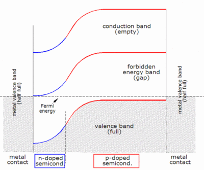
Ohmic metal-semiconductor contacts are made to both the n-type and p-type sides of the solar cell, and the electrodes connected to an external load.
directly, but it can then be solved using the Lambert W function: When an external load is used with the cell, its resistance can simply be added to RS and
Assuming the shunt resistance is high enough to neglect the final term of the characteristic equation, the open-circuit voltage VOC is: Similarly, when the cell is operated at short circuit,
The values of IL, I0, RS, and RSH are dependent upon the physical size of the solar cell.
By the same argument, it will also have half the RS of the series resistance related to vertical current flow; however, for large-area silicon solar cells, the scaling of the series resistance encountered by lateral current flow is not easily predictable since it will depend crucially on the grid design (it is not clear what "otherwise identical" means in this respect).
Since the changes in the currents are the dominating ones and are balancing each other, the open-circuit voltage is practically the same; VOC starts to depend on the cell size only if RSH becomes too low.
Another advantage is that the density equation naturally scales the parameter values to similar orders of magnitude, which can make numerical extraction of them simpler and more accurate even with naive solution methods.
For instance, certain parasitic effects grow in importance as cell sizes shrink and can affect the extracted parameter values.
If volume is the binding constraint, then efficiency density based on surface area may be of less relevance.
The overall effect of temperature on cell efficiency can be computed using these factors in combination with the characteristic equation.
The figure above shows I-V curves that might typically be seen for a crystalline silicon solar cell at various temperatures.
The result is that the current-controlled portion of the I-V curve begins to sag toward the origin, producing a significant decrease in
Very high values of RS will also produce a significant reduction in ISC; in these regimes, series resistance dominates and the behavior of the solar cell resembles that of a resistor.
These effects are shown for crystalline silicon solar cells in the I-V curves displayed in the figure to the right.
The result is that the voltage-controlled portion of the I-V curve begins to sag far from the origin, producing a significant decrease in
Much as in the case of a high series resistance, a badly shunted solar cell will take on operating characteristics similar to those of a resistor.
These effects are shown for crystalline silicon solar cells in the I-V curves displayed in the figure to the right.
This explains mathematically the reason for the reduction in VOC that accompanies increases in temperature described above.
The effect of reverse saturation current on the I-V curve of a crystalline silicon solar cell are shown in the figure to the right.
The ideality factor (also called the emissivity factor) is a fitting parameter that describes how closely the diode's behavior matches that predicted by theory, which assumes the p–n junction of the diode is an infinite plane and no recombination occurs within the space-charge region.
The effect of changing ideality factor independently of all other parameters is shown for a crystalline silicon solar cell in the I-V curves displayed in the figure to the right.
Most solar cells, which are quite large compared to conventional diodes, well approximate an infinite plane and will usually exhibit near-ideal behavior under standard test conditions (n ≈ 1).
Sometimes, the ideality factor is observed to be greater than 2, which is generally attributed to the presence of Schottky diode or heterojunction in the solar cell.
[11] The presence of a heterojunction offset reduces the collection efficiency of the solar cell and may contribute to low fill-factor.