Semiconductor
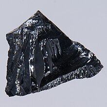
Some examples of semiconductors are silicon, germanium, gallium arsenide, and elements near the so-called "metalloid staircase" on the periodic table.
After silicon, gallium arsenide is the second-most common semiconductor and is used in laser diodes, solar cells, microwave-frequency integrated circuits, and others.
Semiconductor devices can display a range of different useful properties, such as passing current more easily in one direction than the other, showing variable resistance, and having sensitivity to light or heat.
[2] The conductivity of silicon is increased by adding a small amount (of the order of 1 in 108) of pentavalent (antimony, phosphorus, or arsenic) or trivalent (boron, gallium, indium) atoms.
[4] The modern understanding of the properties of a semiconductor relies on quantum physics to explain the movement of charge carriers in a crystal lattice.
The semiconductor materials used in electronic devices are doped under precise conditions to control the concentration and regions of p- and n-type dopants.
[5][8] A difference in electric potential on a semiconducting material would cause it to leave thermal equilibrium and create a non-equilibrium situation.
Such disruptions can occur as a result of a temperature difference or photons, which can enter the system and create electrons and holes.
They are generally used in thin film structures, which do not require material of higher electronic quality, being relatively insensitive to impurities and radiation damage.
Current mass production processes use crystal ingots between 100 and 300 mm (3.9 and 11.8 in) in diameter, grown as cylinders and sliced into wafers.
The silicon wafer is located on the cathode, which causes it to be hit by the positively charged ions that are released from the plasma.
However, one important feature of semiconductors (and some insulators, known as semi-insulators) is that their conductivity can be increased and controlled by doping with impurities and gating with electric fields.
Doping and gating move either the conduction or valence band much closer to the Fermi level and greatly increase the number of partially filled states.
The addition of 0.001% of arsenic (an impurity) donates an extra 1017 free electrons in the same volume and the electrical conductivity is increased by a factor of 10,000.
[35] During manufacture, dopants can be diffused into the semiconductor body by contact with gaseous compounds of the desired element, or ion implantation can be used to accurately position the doped regions.
In 1839, Alexandre Edmond Becquerel reported observation of a voltage between a solid and a liquid electrolyte, when struck by light, the photovoltaic effect.
[41] A unified explanation of these phenomena required a theory of solid-state physics, which developed greatly in the first half of the 20th century.
Karl Baedeker, by observing a Hall effect with the reverse sign to that in metals, theorized that copper iodide had positive charge carriers.
Johan Koenigsberger [de] classified solid materials like metals, insulators, and "variable conductors" in 1914 although his student Josef Weiss already introduced the term Halbleiter (a semiconductor in modern meaning) in his Ph.D. thesis in 1910.
Walter H. Schottky and Nevill Francis Mott developed models of the potential barrier and of the characteristics of a metal–semiconductor junction.
By 1938, Boris Davydov had developed a theory of the copper-oxide rectifier, identifying the effect of the p–n junction and the importance of minority carriers and surface states.
This was later explained by John Bardeen as due to the extreme "structure sensitive" behavior of semiconductors, whose properties change dramatically based on tiny amounts of impurities.
[39] Commercially pure materials of the 1920s containing varying proportions of trace contaminants produced differing experimental results.
A working solar cell, of low efficiency, was constructed by Charles Fritts in 1883, using a metal plate coated with selenium and a thin layer of gold; the device became commercially useful in photographic light meters in the 1930s.
Round observed light emission when electric current passed through silicon carbide crystals, the principle behind the light-emitting diode.
[44][45] In the years preceding World War II, infrared detection and communications devices prompted research into lead-sulfide and lead-selenide materials.
[46] In 1922, Oleg Losev developed two-terminal, negative resistance amplifiers for radio, but he died in the Siege of Leningrad after successful completion.
The first p–n junction in silicon was observed by Russell Ohl about 1941 when a specimen was found to be light-sensitive, with a sharp boundary between p-type impurity at one end and n-type at the other.
[47] In France, during the war, Herbert Mataré had observed amplification between adjacent point contacts on a germanium base.
[48] However, early junction transistors were relatively bulky devices that were difficult to manufacture on a mass-production basis, which limited them to a number of specialised applications.