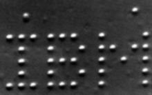
IBM (atoms)
[1] A scanning tunneling microscope was used to arrange 35 individual xenon atoms on a substrate of chilled crystal of nickel to spell out the three letter company initialism.
[2][3] Donald Eigler and Erhard Schweizer of the IBM Almaden Research Center in San Jose, California, discovered the ability using a scanning tunneling microscope (STM) to move atoms about the surface.
[4] In the demonstration, where the microscope was used in low temperature,[5] they positioned 35 individual xenon atoms on a substrate of chilled crystal of nickel to form the acronym "IBM".
They also assembled chains of xenon atoms similar in form to molecules.
[1] The demonstrated capacity showed the potential of fabricating rudimentary structures and allowed insights as to the extent of device miniaturization.