Molecular-beam epitaxy
[1] MBE is used to make diodes and MOSFETs (MOS field-effect transistors) at microwave frequencies, and to manufacture the lasers used to read optical discs (such as CDs and DVDs).
The most important aspect of an MBE process is the deposition rate (typically less than 3,000 nm per hour) that allows the films to grow epitaxially (in layers on top of the existing crystal).
The absence of carrier gases, as well as the ultra-high vacuum environment, result in the highest achievable purity of the grown films.
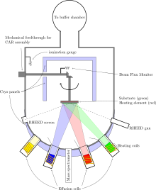
In solid source MBE, elements such as gallium and arsenic, in ultra-pure form, are heated in separate quasi-Knudsen effusion cells or electron-beam evaporators until they begin to slowly sublime.
In other systems, the wafers on which the crystals are grown may be mounted on a rotating platter, which can be heated to several hundred degrees Celsius during operation.
Oxygen sources, for example, can be incorporated for depositing oxide materials for advanced electronic, magnetic and optical applications.
One of the achievements of molecular-beam epitaxy is the nano-structures that permit the formation of atomically flat and abrupt hetero-interfaces.
[8] These heterostructure nanowire lasers are only possible to build using advanced MBE techniques, allowing monolithical integration on silicon[9] and picosecond signal processing.