Nano-FTIR
A typical nano-FTIR setup thus consists of an atomic force microscope, a broadband infrared light source used for tip illumination, and a Michelson interferometer acting as Fourier-transform spectrometer.
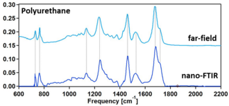
The use of broadband infrared sources enables the acquisition of continuous spectra, which is a distinctive feature of nano-FTIR compared to s-SNOM.
Nano-FTIR is capable of performing infrared (IR) spectroscopy of materials in ultrasmall quantities and with nanoscale spatial resolution.
[4] For organic compounds, polymers, biological and other soft matter, nano-FTIR spectra can be directly compared to the standard FTIR databases, which allows for a straightforward chemical identification and characterization.
It uses an AFM operated in noncontact mode that is intrinsically nondestructive and sufficiently gentle to be suitable for soft-matter and biological sample investigations.
Nano-FTIR can be utilized from THz to visible spectral range (and not only in infrared as its name suggests) depending on the application requirements and availability of broadband sources.
Nano-FTIR is complementary to tip-enhanced Raman spectroscopy (TERS), SNOM, AFM-IR and other scanning probe methods that are capable of performing vibrational analysis.
Nano-FTIR is based on s-SNOM, where the infrared beam from a light source is focused onto a sharp, typically metalized AFM tip and the backscattering is detected.
It boosts the weak near-field signal due to interference with the strong reference field, helps to eliminate the background caused by parasitic scattering off everything that falls into large diffraction-limited beam focus, and most importantly, allows for recording of both amplitude s and phase φ spectra of the tip-scattered radiation.
Nano-FTIR was first described in 2005 in a patent by Ocelic and Hillenbrand as Fourier-transform spectroscopy of tip-scattered light with an asymmetric spectrometer (i.e. the tip/sample placed inside one of the interferometer arms).
[11] The first realization of s-SNOM with FTIR was demonstrated in 2006 in the laboratory of F. Keilmann using a mid-infrared source based on a simple version of nonlinear difference-frequency generation (DFG).
[12] However, the mid-IR spectra in this realization were recorded using dual comb spectroscopy principles,[13][14] yielding a discrete set of frequencies and thus demonstrating a multiheterodyne imaging technique rather than nano-FTIR.
The first continuous spectra were recorded only in 2009 in the same laboratory using a supercontinuum IR beam also obtained by DFG in GaSe upon superimposing two pulsed trains emitted from Er-doped fiber laser.
[20] Additional boost to the development of nano-FTIR came from the utilization of the synchrotron radiation that provide extreme bandwidth, yet at the expense of weaker IR spectral irradiance compared to broadband laser sources.
[11] The detection module optimized for broadband illumination sources was first made available in 2010 as a part of the standard neaSNOM microscope system.
The same year the development of a cryo-neaSNOM – the first system of its kind to enable nanoscale near-field imaging & spectroscopy at cryogenic temperatures – was announced.
[28] Nano-FTIR brings the spatial resolution to 10-20 nm scale (vs. ~2-5 μm in microspectroscopy), which has been utilized for broadband spatially-resolved spectroscopy of crystalline[24][25] and phase-change[29] materials, semiconductors,[27] minerals,[30] biominerals and proteins.
[26] Nano-FTIR is highly suitable for performing local ultrafast pump-probe spectroscopy due to intereferometric detection and an intrinsic ability to vary the probe delay time.
It has been applied for studies of ultrafast nanoscale plasmonic phenomena in Graphene,[31][32] for performing nanospectroscopy of InAs nanowires with subcycle resolution[33] and for probing the coherent vibrational dynamics of nanoscopic ensembles.
[6] The availability of both amplitude and phase of the scattered field and theoretically well understood signal formation in nano-FTIR allow for the recovery of both real and imaginary parts of the dielectric function, i.e. finding the index of refraction and the extinction coefficient of the sample.
One of such approaches is based on the Taylor expansion of the scattered field with respect to a small parameter that isolates the dielectric properties of the sample and allows for a polynomial representation of measured near-field contrast.
can be determined as a solution of a simple polynomial equation[36] Near-field methods, including nano-FTIR, are typically viewed as a technique for surface studies due to short probing ranges of about couple tip radii (~20-50 nm).
However it has been demonstrated that within such probing ranges, s-SNOM is capable of detecting subsurface features to some extents,[37][38][39][40] which could be used for the investigations of samples capped by thin protective layers,[41] or buried polymers,[42][43] among others.
This is often achieved by a simple method of utilizing signals recorded at multiple demodulation orders naturally returned by nano-FTIR in the process of background suppression.
[44] This way, nano-FTIR has a demonstrated capability for the recovery of thickness and permittivity of layered films and nanostructures,[44] which has been utilized for the nanoscale depth profiling of multiphase materials[45] and high-Tc cuprate nanoconstriction devices patterned by focused ion beams.
[46] In other words, nano-FTIR has a unique capability of recovering the same information about thin-film samples that is typically returned by ellipsometry or impedance spectroscopy, yet with nanoscale spatial resolution.
Nano-FTIR is compatible with cryogenic s-SNOM that has already been utilized for reveling a nanotextured coexistence of metal and correlated Mott insulator phases in Vanadium oxide near the metal-insulator transition.
[45] Nano-FTIR has a plenitude of applications,[51] including polymers and polymer composites,[4] organic films,[52] semiconductors,[16][26][27][46] biological research (cell membranes, proteins structure, studies of single viruses),[2][26][53] chemistry and catalysis,[54] photochemistry,[55] minerals and biominerals,[53][26][30] geochemistry,[56] corrosion[57] and materials sciences,[5][23] low-dimensional materials,[58][32] photonics,[59][26] energy storage,[45] cosmetics, pharmacology and environmental sciences.
The background is nearly insensitive to small variations of the tip height and is nearly eliminated for sufficiently high demodulation orders (typically
This way, besides providing the interferometric gain, the asymmetric interferometer utilized in nano-FTIR also eliminates the multiplicative background, which otherwise could be a source of various artifacts and is often overlooked in other s-SNOM based spectroscopies.