Quantum point contact
A quantum point contact (QPC) is a narrow constriction between two wide electrically conducting regions, of a width comparable to the electronic wavelength (nano- to micrometer).
[1] The importance of QPC lies in the fact that they prove quantisation of ballistic conductance in mesoscopic systems.
[3] They are based on earlier work by the British group which showed how split gates could be used to convert a two-dimensional electron gas into one-dimension, first in silicon[4] and then in gallium arsenide.
The zero-field conductance quantisation and the smooth transition to the quantum Hall effect on applying a magnetic field are essentially consequences of the equipartition of current among an integer number of propagating modes in the constriction.
In a more controlled way, quantum point contacts are formed in a two-dimensional electron gas (2DEG), e.g. in GaAs/AlGaAs heterostructures.
By applying a voltage to suitably shaped gate electrodes, the electron gas can be locally depleted and many different types of conducting regions can be created in the plane of the 2DEG, among them quantum dots and quantum point contacts.
Another means of creating a QPC is by positioning the tip of a scanning tunneling microscope close to the surface of a conductor.
Geometrically, a quantum point contact is a constriction in the transverse direction which presents a resistance to the motion of electrons.
However, there is a fundamental difference here resulting from the small system size which requires a quantum mechanical analysis.
This way the geometric constriction of the point contact turns the conductance through the opening to a one dimensional system.
Moreover, it requires a quantum mechanical description of the system that results in the quantisation of conductance.
Quantum mechanically, the current through the point contact is equipartitioned among the 1D subands, or transverse modes, in the constriction.
It is important to state that the previous discussion does not take into account possible transitions among modes.
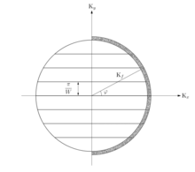
is the transition matrix which incorporates non-zero probabilities of transmission from mode n to m. At low temperatures and voltages, unscattered and untrapped electrons contributing to the current have a certain energy/momentum/wavelength called Fermi energy/momentum/wavelength.
The waveguide analogy is applicable as long as coherence is not lost through scattering, e.g., by a defect or trapping site.
The current carried by such a quantum state is the product of the velocity times the electron density.
As a function of the width of the point contact (or gate voltage in the case of GaAs/AlGaAs heterostructure devices), the conductance shows a staircase behavior as more and more modes (or channels) contribute to the electron transport.
On increasing the temperature, one finds experimentally that the plateaux acquire a finite slope until they are no longer resolved.
[9] An external magnetic field applied to the quantum point contact lifts the spin degeneracy and leads to half-integer steps in the conductance.
is independent of the width of the constriction, given by the theory of the quantum Hall effect.
Anomalous features on the quantized conductance steps are often observed in transport measurements of quantum point contacts.
Quasi-bound states arising from impurities, charge traps, and reflections within the constriction may also result in conductance structure close to the 1D limit.
Since the conductance through the contact strongly depends on the size of the constriction, any potential fluctuation (for instance, created by other electrons) in the vicinity will influence the current through the QPC.
[11][12][13][14] In device physics, the configuration of QPCs is used for demonstrating a fully ballistic field-effect transistor.
A nickel wire is brought close enough to a gold surface and then, by the use of a piezoelectric actuator, the distance between the wire and the surface can be changed and thus, the transport characteristics of the device change between electron tunneling and ballistic.