Electron backscatter diffraction
EBSD is used for impurities and defect studies, plastic deformation, and statistical analysis for average misorientation, grain size, and crystallographic texture.
[4][5] A high-energy electron beam (typically 20 kV) is focused on a small volume and scatters with a spatial resolution of ~20 nm at the specimen surface.
[17][18] The systematically arranged Kikuchi bands, which have a range of intensity along their width, intersect around the centre of the regions of interest (ROI), describing the probed volume crystallography.
It is typically mounted using a conductive compound (e.g. an epoxy thermoset filled with Cu), which minimises image drift and sample charging under electron beam irradiation.
Typically the sample is ground using SiC papers from 240 down to 4000 grit, and polished using diamond paste (from 9 to 1 μm) then in 50 nm colloidal silica.
[26] Usual settings for high-quality EBSPs are 15 nA current, 20 kV beam energy, 18 mm working distance, long exposure time, and minimal CCD pixel binning.
[27][28][29][30] The EBSD phosphor screen is set at an 18 mm working distance and a map's step size of less than 0.5 μm for strain and dislocations density analysis.
[37] In contrast, Isabell and David[40] concluded that depth resolution in homogeneous crystals could also extend up to 1 μm due to inelastic scattering (including tangential smearing and channelling effect).
[46][47] Both the EBSD experiment and simulations typically make two assumptions: that the surface is pristine and has a homogeneous depth resolution; however, neither of them is valid for a deformed sample.
[37] If the setup geometry is well described, it is possible to relate the bands present in the diffraction pattern to the underlying crystal and crystallographic orientation of the material within the electron interaction volume.
[57] Overall, indexing diffraction patterns in EBSD involves a complex set of algorithms and calculations, but is essential for determining the crystallographic structure and orientation of materials at a high spatial resolution.
[50] While this geometric description related to the kinematic solution using the Bragg condition is very powerful and useful for orientation and texture analysis, it only describes the geometry of the crystalline lattice.
Later developments involved exploiting various geometric relationships between the generation of an EBSP and the chamber geometry (shadow casting and phosphor movement).
Thus, most commercial EBSD systems use the indexing algorithm combined with an iterative movement of crystal orientation and suggested pattern centre location.
Thus, scanning the electron beam in a prescribed fashion (typically in a square or hexagonal grid, correcting for the image foreshortening due to the sample tilt) results in many rich microstructural maps.
[73] Microscope misalignment, image shift, scan distortion that increases with decreasing magnification, roughness and contamination of the specimen surface, boundary indexing failure and detector quality can lead to uncertainties in determining the crystal orientation.
[74] The EBSD signal-to-noise ratio depends on the material and decreases at excessive acquisition speed and beam current, thereby affecting the angular resolution of the measurement.
Measuring strain at the microscale requires careful consideration of other key details besides the change in length/shape (e.g., local texture, individual grain orientations).
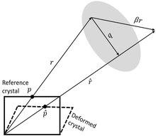
[1] Cross-correlation-based, high angular resolution electron backscatter diffraction (HR-EBSD) – introduced by Wilkinson et al.[83][84] – is an SEM-based technique to map relative elastic strains and rotations, and estimate the geometrically necessary dislocation (GND) density in crystalline materials.
In practice, pattern shifts are measured in more than 20 ROI per EBSP to find a best-fit solution to the deformation gradient tensor, representing the relative lattice distortion.
), and the relationship is simplified; thus, eight out of the nine displacement gradient tensor components can be calculated by measuring the shift at four distinct, widely spaced regions on the EBSP.
) is zero (i.e., traction-free surface[88]), and using Hooke's law with anisotropic elastic stiffness constants, the missing ninth degree of freedom can be estimated in this constrained minimisation problem by using a nonlinear solver.
To address this problem, Ruggles et al.[94] improved the HR-EBSD precision, even at 12° of lattice rotation, using the inverse compositional Gauss–Newton-based (ICGN) method instead of cross-correlation.
For simulated patterns, Vermeij and Hoefnagels[95] also established a method that achieves a precision of ±10−5 in the displacement gradient components using a full-field integrated digital image correlation (IDIC) framework instead of dividing the EBSPs into small ROIs.
However, selecting the reference pattern (EBSP0) plays a key role, as severely deformed EBSP0 adds phantom lattice distortions to the map values, thus, decreasing the measurement precision.
Nevertheless, VFSD images do not include the quantitative information inherent to traditional EBSD maps; they simply offer representations of the microstructure.
[48][137] EBSD, when used together with other in-SEM techniques such as cathodoluminescence (CL),[138] wavelength dispersive X-ray spectroscopy (WDS)[139] and/or EDS can provide a deeper insight into the specimen's properties and enhance phase identification.
[140][141] For example, the minerals calcite (limestone) and aragonite (shell) have the same chemical composition – calcium carbonate (CaCO3) therefore EDS/WDS cannot tell them apart, but they have different microcrystalline structures so EBSD can differentiate between them.
The serial sectioning can be performed using a variety of methods, including mechanical polishing,[156] focused ion beam (FIB) milling,[157] or ultramicrotomy.
[158] The choice of sectioning method depends on the size and shape of the sample, on its chemical composition, reactivity and mechanical properties, as well as the desired resolution and accuracy of the 3D map.