Single-layer materials
[1][2] The atomic structure and calculated basic properties of these and many other potentially synthesisable single-layer materials, can be found in computational databases.
[7] Andre Geim and Konstantin Novoselov won the 2010 Nobel Prize in Physics "for groundbreaking experiments regarding the two-dimensional material graphene".
First-principle calculations using phonon dispersion curves and ab-initio finite temperature, quantum mechanical molecular dynamics simulations showed graphyne and its boron nitride analogues to be stable.
[16][verification needed] Later during 2022 synthesis of multi-layered γ‑graphyne was successfully performed through the polymerization of 1,3,5-tribromo-2,4,6-triethynylbenzene under Sonogashira coupling conditions.
First predicted by theory in the mid-1990s in a freestanding state,[21] and then demonstrated as distinct monoatomic layers on substrates by Zhang et al.,[22] different borophene structures were experimentally confirmed in 2015.
[33] Its buckled structure leads to high reactivity against common air pollutants such as NOx and COx and it is able to trap and dissociate them at low temperature.
Theoretical calculations[40] predicted that antimonene would be a stable semiconductor in ambient conditions with suitable performance for (opto)electronics.
[42] In a study made in 2018,[43] antimonene modified screen-printed electrodes (SPE's) were subjected to a galvanostatic charge/discharge test using a two-electrode approach to characterize their supercapacitive properties.
The same study also depicts the in-situ production of antimonene oxide/PEDOT:PSS nanocomposites as electrocatalytic platforms for the determination of nitroaromatic compounds.
[51][52] Emdadul et al.[53] predicted the mechanical strength and phonon thermal conductivity of monolayer β-bismuthene through atomic-scale analysis.
In addition, their predicted phonon thermal conductivity of ~1.3 W/m∙K at 300 K is considerably lower than other analogous 2D honeycombs, making it a promising material for thermoelectric operations.
On 16 April 2024, scientists from Linköping University in Sweden reported that they had produced goldene, a single layer of gold atoms 100nm wide.
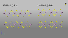
Because the structure consists of in-plane covalent bonds and inter-layer van der Waals interactions, the electronic properties of monolayer TMDs are highly anisotropic.
As with other two-dimensional materials, properties can be highly geometry-dependent; the surface of MoS2 is catalytically inactive, but the edges can act as active sites for catalyzing reactions.
From this material, the calcium (Ca) is removed by de-intercalation with HCl to give a layered solid with the empirical formula GeH.
SLSiN (acronym for Single-Layer Silicon Nitride), a novel 2D material introduced as the first post-graphene member of Si3N4, was first discovered computationally in 2020 via density-functional theory based simulations.
[87] Using melamine (carbon and nitrogen ring structure) as a monomer, researchers created 2DPA-1, a 2-dimensional polymer sheet held together by hydrogen bonds.
One of the first reports of bilayer graphene was in the seminal 2004 Science paper by Geim and colleagues, in which they described devices "which contained just one, two, or three atomic layers".
[96] Nanoindentation testing is commonly used to experimentally measure elastic modulus, hardness, and fracture strength of 2D materials.
From these directly measured values, models exist which allow the estimation of fracture toughness, work hardening exponent, residual stress, and yield strength.
The strip geometry is difficult to prepare but allows for easier analysis due to linear resulting stress fields.
Elastic modulus and residual stress values can be extracted by determining the linear and cubic portions of the experimental force-displacement curve.
[101][102] Fracture toughness of 2D materials in Mode I (KIC) has been measured directly by stretching pre-cracked layers and monitoring crack propagation in real-time.
The major expectation held amongst researchers is that given their exceptional properties, 2D materials will replace conventional semiconductors to deliver a new generation of electronics.
2D nanoparticles such as carbon-based 2D materials, silicate clays, transition metal dichalcogenides (TMDs), and transition metal oxides (TMOs) provide enhanced physical, chemical, and biological functionality owing to their uniform shapes, high surface-to-volume ratios, and surface charge.
[106] 2D nanomaterials are highly diverse in terms of their mechanical, chemical, and optical properties, as well as in size, shape, biocompatibility, and degradability.
[107][108] These diverse properties make 2D nanomaterials suitable for a wide range of applications, including drug delivery, imaging, tissue engineering, biosensors, and gas sensors among others.
This characteristic makes these materials invaluable for applications requiring high levels of surface interactions on a small scale.
Despite the rapid pace of development in the field of 2D nanomaterials, these materials must be carefully evaluated for biocompatibility in order to be relevant for biomedical applications.
Additionally, the complexities of variable particle size and shape, impurities from manufacturing, and protein and immune interactions have resulted in a patchwork of knowledge on the biocompatibility of these materials.

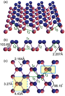
36 cluster might be seen as smallest borophene; front and side view