Transition metal dichalcogenide monolayers
The key feature of these materials is the interaction of large atoms in the 2D structure as compared with first-row transition-metal dichalcogenides, e.g., WTe2 exhibits anomalous giant magnetoresistance and superconductivity.
[1] The discovery of graphene shows how new physical properties emerge when a bulk crystal of macroscopic dimensions is thinned down to one atomic layer.
[7][8][9] TMDs are often combined with other 2D materials like graphene and hexagonal boron nitride to make van der Waals heterostructures.
Two important consequences of that are: These properties indicate that TMD monolayers represent a promising platform to explore spin and valley physics with the corresponding possible applications.
TMD monolayers might be an alternative: they are structurally stable, display a band gap and show electron mobilities comparable to those of silicon, so they can be used to fabricate transistors.
[29] Unlike in bulk samples it is much more difficult to uniformly deform 2D monolayers of material and as a result, taking mechanical measurements of 2D systems is more challenging.
[30] Through this method, defect free mechanically exfoliated monolayer flakes of MoS2 were found to have a Young's modulus of 270 GPa with a maximum experienced strain of 10% before breaking.
[31] In the same study, it was found that bilayer mechanically exfoliated MoS2 flakes have a lower Young's modulus of 200 GPa, which is attributed to interlayer sliding and defects in the monolayer.
[45] Geometrically confined-growth techniques are also recently applied to realize wafer-scale single-domain TMD monolayer arrays and their heterostructures.
[46] Molecular-beam epitaxy (MBE) is an established technique for growing semiconductor devices with atomic monolayer thickness control.
MBE has been used to grow different TMDs, such as MoSe2, WSe2, and early transition metals, including titanium, vanadium, and chromium, tellurides,[47][48][49] resulting in extremely clean samples with a thickness of only 0.5 monolayer.
Precursors for the target materials are placed into evaporation cells, usually as powder (for example selenium), or as a rod (for example molybdenum).
[47][52] The improvement in sample quality is considerable when compared to exfoliation, as MBE is more effective in getting rid of the large flakes and impurities.
[57] A strategy for colloidal synthesis from soluble transistion metal and sulfur precursors was found recently, yielding highly defined nanoplatelets and nanosheets with a thickness of 1-2 monolayers.
This degree of freedom opens up a new field of physics: the controlling of carriers k-valley index, also called valleytronics.
Indeed, the reduced dielectric screening and the quantum size effect present in these ultrathin materials make the binding energy of excitons much stronger than those in traditional semiconductors.
The main difference is that this system is not stable and tends to relax to the vacuum state, which is here represented by an electron in the valence band.
This is the energy of the photons emitted by TMD monolayers and observed as huge emission peaks in photoluminescence (PL) experiments, such as the one labelled X0 in the figure.
The analogy with hydrogen atom doesn't stop here as excitonic excited states were observed at higher energies and with different techniques.
As a consequence the optical gap for B-exciton is larger and the corresponding peak is found at higher energy in PL and reflectivity measurements.
Another peak usually appears in the PL spectra of TMD monolayers, which is associated to different quasi-particles called trions.
It is believed now that this doping is extrinsic, which means that it arises from charged trap states present in the substrate (generally SiO2).
Positioning a TMD monolayer between two flakes of hBN removes this extrinsic doping and greatly increase the optical quality of the sample.
[77][78][79][80][81][82] Common forms of radiation used to create defects in TMDs are particle and electromagnetic irradiation, impacting the structure and electronic performance of these materials.
[83] Damage to this unique class of materials occurs mainly through sputtering and displacement for metals or radiolysis and charging for insulators and semiconductors.
[87] A new type of asymmetric transitional metal dichalcogenide, the Janus TMDs monolayers, has been synthesized by breaking the out-of-plane structural symmetry via plasma assisted chemical vapor deposition.
The top layer of sulfur atoms on MoS2 is stripped using hydrogen ions, forming an intermediate state, MoSH.
[88] A field-effect transistor (FET) made of monolayer MoS2 showed an on/off ratio exceeding 108 at room temperature owing to electrostatic control over the conduction in the 2D channel.
[111][112][113] The advantage that this technique offers in producing 2D materials is its spatial growth selectivity and its ability to deposit over 3D surfaces.
As an application in electronics, its field-effect transistors has been realised using its few layers as a conducting channel material offering a high current modulation ratio larger than 10000 at room temperature.

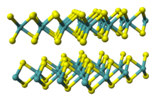


2 , with Mo in blue and S in yellow


2 structure
