Through-hole technology
This is because of difficulties in use with automated component placement machinery, and poorer reliability because of reduced vibration and mechanical shock resistance in the completed assembly.
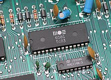
For electronic components with two or more leads, for example, diodes, transistors, ICs, or resistor packs, a range of standard-sized semiconductor packages are used, either directly onto the PCB or via a socket.
While through-hole mounting provides strong mechanical bonds when compared to SMT techniques, the additional drilling required makes the boards more expensive to produce.
[4] Design engineers often prefer the larger through-hole rather than surface mount parts when prototyping, because they can be easily used with breadboard sockets.
However, high-speed or high-frequency designs may require SMT technology to minimize stray inductance and capacitance in wire leads, which would impair circuit function.