Transmission electron microscopy
This enables the instrument to capture fine detail—even as small as a single column of atoms, which is thousands of times smaller than a resolvable object seen in a light microscope.
The research team worked on lens design and CRO column placement, to optimize parameters to construct better CROs, and make electron optical components to generate low magnification (nearly 1:1) images.
[8] Knoll's research group was unaware of this publication until 1932, when they realized that the de Broglie wavelength of electrons was many orders of magnitude smaller than that for light, theoretically allowing for imaging at atomic scales.
Further work on the electron microscope was hampered by the destruction of a new laboratory constructed at Siemens by an air raid, as well as the death of two of the researchers, Heinz Müller and Friedrick Krause during World War II.
Crewe and coworkers at the University of Chicago developed the cold field electron emission source and built a STEM able to visualize single heavy atoms on thin carbon substrates.
Variable apertures after the sample allow the user to select the range of spatial positions or electron scattering angles to be used in the formation of an image or a diffraction pattern.
To increase the mean free path of the electron gas interaction, a standard TEM is evacuated to low pressures, typically on the order of 10−4 Pa.[33] The need for this is twofold: first the allowance for the voltage difference between the cathode and the ground without generating an arc, and secondly to reduce the collision frequency of electrons with gas atoms to negligible levels—this effect is characterized by the mean free path.
TEM components such as specimen holders and film cartridges must be routinely inserted or replaced requiring a system with the ability to re-evacuate on a regular basis.
To accommodate this, the TEM stage allows movement of the sample in the XY plane, Z height adjustment, and commonly a single tilt direction parallel to the axis of side entry holders.
The design criteria of TEM stages are complex, owing to the simultaneous requirements of mechanical and electron-optical constraints and specialized models are available for different methods.
[36] Earlier designs of TEM accomplished this with a complex set of mechanical downgearing devices, allowing the operator to finely control the motion of the stage by several rotating rods.
The coils can contain a variable current, but typically use high voltages, and therefore require significant insulation in order to prevent short-circuiting the lens components.
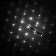
Analysis of diffraction patterns beyond point-position can be complex, as the image is sensitive to a number of factors such as specimen thickness and orientation, objective lens defocus, and spherical and chromatic aberration.
This normally results in chromatic aberration – however this effect can, for example, be used to generate an image which provides information on elemental composition, based upon the atomic transition during electron-electron interaction.
Using focused ion beam milling, a new technique has been proposed[48] which uses pillar-shaped specimen and a dedicated on-axis tomography holder to perform 180° rotation of the sample inside the pole piece of the objective lens in TEM.
Unlike neutron or X-ray radiation the electrons in the beam interact readily with the sample, an effect that increases roughly with atomic number squared (Z2).
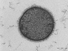
Biological specimens may be embedded in resin to withstand the high vacuum in the sample chamber and to enable cutting tissue into electron transparent thin sections.
Compounds of heavy metals such as osmium, lead, uranium or gold (in immunogold labelling) may be used prior to TEM observation to selectively deposit electron dense atoms in or on the sample in desired cellular or protein region.
The TEM images taken in plan view rather than cross-section reveal that the MgO layer within MTJs contains a large number of grain boundaries that may be diminishing the properties of devices.
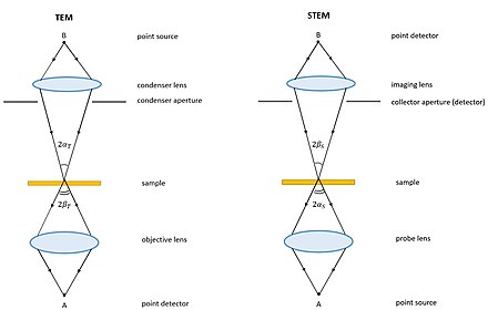
A TEM can be modified into a scanning transmission electron microscope (STEM) by the addition of a system that rasters a convergent beam across the sample to form the image, when combined with suitable detectors.
[65] Types of in-situ experiments include studying nanomaterials,[66] biological specimens, chemical reactions of molecules,[67] liquid-phase electron microscopy,[68][69] and material deformation testing.
Additionally, coarsening and grain growth, along with other diffusion-related processes occur more rapidly at elevated temperatures, where kinetics are improved, allowing for the observation of related phenomena under transmission electron microscopy within reasonable time scales.
However, due to the geometry of most TEMs, inserting large in-situ holders requires the user to compromise the objective lens and endure spherical aberrations.
By simultaneously observing deformation phenomena and measuring mechanical response in situ, it is possible to connect nano-mechanical testing information to models that describe both the subtlety and complexity of how materials respond to stress and strain.
In order to study the temperature-dependent mechanical properties of TEM samples, the holder can be cooled through a cold finger connected to a liquid nitrogen reservoir.
[88] For nanoindentation experiments, TEM samples are typically shaped as wedges using a tripod polisher, H-bar window or a micro-nanopillar using focused ion beam to create enough space for a tip to be pressed at the desired electron transparent location.
[90] Micro Electro-Mechanical Systems (MEMs) based holders provide a cheap and customizable platform to conduct mechanical tests on previously difficult samples to work with such as micropillars, nanowires, and thin films.
[93] Much of current research focuses on developing sample holders that can perform mechanical tests while creating an environmental stimulus such as temperature change, variable strain rates, and different gas environments.
In addition, the emergence of high resolution detectors are allowing to monitor dislocation motion and interactions with other defects and pushing the limits of sub-nanometre strain measurements.
By combining multiple images with different spatial frequencies, the use of techniques such as focal series reconstruction can be used to improve the resolution of the TEM in a limited manner.