Dynamic random-access memory
To prevent this, DRAM requires an external memory refresh circuit which periodically rewrites the data in the capacitors, restoring them to their original charge.
In contrast, SRAM, which is faster and more expensive than DRAM, is typically used where speed is of greater concern than cost and size, such as the cache memories in processors.
[3] In 2018, a "key characteristic of the DRAM market is that there are currently only three major suppliers — Micron Technology, SK Hynix and Samsung Electronics" that are "keeping a pretty tight rein on their capacity".
The cryptanalytic machine code-named Aquarius used at Bletchley Park during World War II incorporated a hard-wired dynamic memory.
This was a radical advance, effectively halving the number of address lines required, which enabled it to fit into packages with fewer pins, a cost advantage that grew with every jump in memory size.
DRAM is usually arranged in a rectangular array of charge storage cells consisting of one capacitor and transistor per data bit.
The quoted number is the clearest way to compare between the performance of different DRAM memories, as it sets the slower limit regardless of the row length or page size.
In the 2000s, manufacturers were sharply divided by the type of capacitor used in their DRAMs and the relative cost and long-term scalability of both designs have been the subject of extensive debate.
The advantage the COB variant possesses is the ease of fabricating the contact between the bitline and the access transistor's source as it is physically close to the substrate surface.
However, this requires the active area to be laid out at a 45-degree angle when viewed from above, which makes it difficult to ensure that the capacitor contact does not touch the bitline.
1T DRAM is a "capacitorless" bit cell design that stores data using the parasitic body capacitance that is inherent to silicon on insulator (SOI) transistors.
This gives 1T DRAM cells the greatest density as well as allowing easier integration with high-performance logic circuits since they are constructed with the same SOI process technologies.
DRAM cells are laid out in a regular rectangular, grid-like pattern to facilitate their control and access via wordlines and bitlines.
Differential sense amplifiers work by driving their outputs to opposing extremes based on the relative voltages on pairs of bitlines.
The disadvantage that caused the near disappearance of this architecture is the inherent vulnerability to noise, which affects the effectiveness of the differential sense amplifiers.
To minimize area overhead, engineers select the simplest and most area-minimal twisting scheme that is able to reduce noise under the specified limit.
As process technology improves to reduce minimum feature sizes, the signal to noise problem worsens, since coupling between adjacent metal wires is inversely proportional to their pitch.
The defective rows and columns are physically disconnected from the rest of the array by a triggering a programmable fuse or by cutting the wire by a laser.
Electrical or magnetic interference inside a computer system can cause a single bit of DRAM to spontaneously flip to the opposite state.
The majority of one-off ("soft") errors in DRAM chips occur as a result of background radiation, chiefly neutrons from cosmic ray secondaries, which may change the contents of one or more memory cells or interfere with the circuitry used to read/write them.
[46] The extra memory bits are used to record parity and to enable missing data to be reconstructed by error-correcting code (ECC).
Laptop computers, game consoles, and specialized devices may have their own formats of memory modules not interchangeable with standard desktop parts for packaging or proprietary reasons.
The Zilog Z80 is perhaps the best known example, as it has an internal row counter R which supplies the address for a special refresh cycle generated after each instruction fetch.
[59] In other systems, especially home computers, refresh was handled by the video circuitry as a side effect of its periodic scan of the frame buffer.
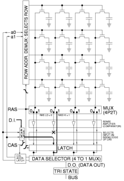
If the CAS line is driven low before RAS (normally an illegal operation), then the DRAM ignores the address inputs and uses an internal counter to select the row to open.
The most significant change, and the primary reason that SDRAM has supplanted asynchronous RAM, is the support for multiple internal banks inside the DRAM chip.
By alternating banks, a single SDRAM device can keep the data bus continuously busy, in a way that asynchronous DRAM cannot.
Graphics RAMs are asynchronous and synchronous DRAMs designed for graphics-related tasks such as texture memory and framebuffers, found on video cards.
WRAM offered up to 25% greater bandwidth than VRAM and accelerated commonly used graphical operations such as text drawing and block fills.
Their primary characteristics are higher clock frequencies for both the DRAM core and I/O interface, which provides greater memory bandwidth for GPUs.