Chemistry of photolithography
Photolithography makes this process possible through the combined use of hexamethyldisilazane (HMDS), photoresist (positive or negative), spin coating, photomask, an exposure system and other various chemicals.
[1] The chemical interaction between all the different components and the surface of the silicon wafer makes photolithography an interesting chemistry problem.
This is done through the process of Czochralski growth, which is diagramed in the adjacent image, and produces a single intact diamond cubic silicon crystal.
Using miller indexes to denote the different plane orientations, the (1,0,0) and the (1,1,1) faces are typically used in silicon wafers (see image).
A table on the right depicts the surface energies, atomic densities, and interatomic spacing of the three planes for a silicon crystal.
The mask allows for precise control over the doping and etching processes used to form devices on silicon wafers.
The compound is applied to the silicon wafer in liquid form and polymerization is controlled through exposure to light.
In order to reliably create small features, the surface of the silicon wafer must be made hydrophobic to promote photoresist adhesion.
Positive photoresists are composed of a novolac resin, ethyl lactate solvent, and Diazonaphthaquinone (DQ) as the photoactive compound.
[9] Positive photoresist reacts with light to cause the polymer to break down and become soluble in a developer solution.
Negative photoresists are composed of a poly(cis-isoprene) matrix, xylene solvent, and bis-arylazide as the photoactive compound.
[10] The wafer can undergo a dehydration bake to remove adsorbed water, and followed by the HMDS treatment also known as the priming stage.
The HMDS promotes good photoresist-to-wafer adhesion because it ensures the wafer surface is hydrophobic.
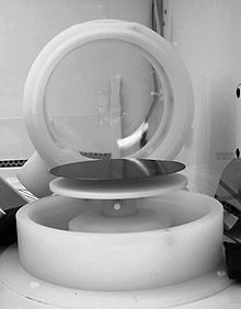
A common issue in spin coating is a "beading" up of solvent at the edge of the silicon wafer.
Currently engineers and scientist are working on figuring out a better way to apply photoresist to the substrate of a silicon wafer.
Spray coating is still in its development phase and much more research needs to be done to make it cost effective and applicable.