Photoresist
A photoresist (also known simply as a resist) is a light-sensitive material used in several processes, such as photolithography and photoengraving, to form a patterned coating on a surface.
To explain this in graphical form you may have a graph on Log exposure energy versus fraction of resist thickness remaining.
[citation needed] In the deep ultraviolet (DUV) spectrum, the π-π* electronic transition in benzene[9] or carbon double-bond chromophores appears at around 200 nm.
Secondary electrons generated by primary ionizing radiation have energies sufficient to dissociate this bond, causing scission.
[13] The primary properties of the photoresist are resolution capability, process dose and focus latitudes required for curing, and resistance to reactive ion etching.
[14]: 966 [15] Other key properties are sensitivity, compatibility with tetramethylammonium hydroxide (TMAH), adhesion, environmental stability, and shelf life.
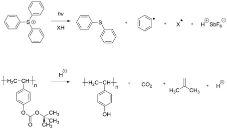
[14]: 966 [15] Photoresists used in production for DUV and shorter wavelengths require the use of chemical amplification to increase the sensitivity to the exposure energy.
[16] Acid diffusion is important not only to increase photoresist sensitivity and throughput, but also to limit line edge roughness due to shot noise statistics.
DNQ-novolac resists are developed by dissolution in a basic solution (usually 0.26N tetramethylammonium hydroxide (TMAH) in water).
As such, it is often used in applications where a permanent resist pattern (one that is not strippable, and can even be used in harsh temperature and pressure environments) is needed for a device.
SU-8 is prone to swelling at smaller feature sizes, which has led to the development of small-molecule alternatives that are capable of obtaining higher resolutions than SU-8.
[24] In 2016, OSTE Polymers were shown to possess a unique photolithography mechanism, based on diffusion-induced monomer depletion, which enables high photostructuring accuracy.
The OSTE polymer material was originally invented at the KTH Royal Institute of Technology, but is now sold by Mercene Labs.
Generally, in this techniques, an elastomeric stamp is used to generate two-dimensional patterns, through printing the “ink” molecules onto the surface of a solid substrate.
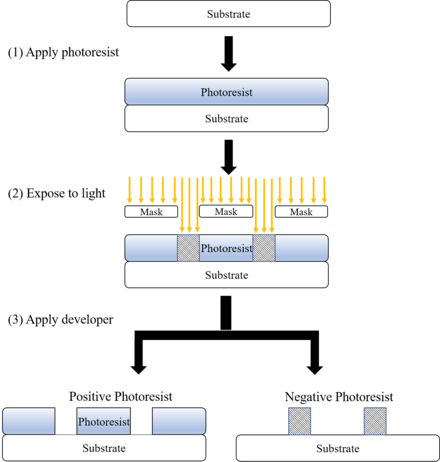
Photolithography allows the complex wiring of an electronic system to be rapidly, economically, and accurately reproduced as if run off a printing press.
The general process is applying photoresist, exposing image to ultraviolet rays, and then etching to remove the copper-clad substrate.
[28] This includes specialty photonics materials, MicroElectro-Mechanical Systems (MEMS), glass printed circuit boards, and other micropatterning tasks.