Atomic force microscopy
Atomic force microscopy[1] (AFM) gathers information by "feeling" or "touching" the surface with a mechanical probe.
This is achieved by raster scanning the position of the sample with respect to the tip and recording the height of the probe that corresponds to a constant probe-sample interaction (see § Topographic image for more).
[3] Subatomic resolution (i.e. the ability to resolve structural details within the electron density of a single atom) has also been achieved by AFM.
Therefore, it does not suffer from a limitation in spatial resolution due to diffraction and aberration, and preparing a space for guiding the beam (by creating a vacuum) and staining the sample are not necessary.
Although SNOM and STED use visible, infrared or even terahertz light to illuminate the sample, their resolution is not constrained by the diffraction limit.
The detector (5) of AFM measures the deflection (displacement with respect to the equilibrium position) of the cantilever and converts it into an electrical signal.
This feedback loop has the cantilever deflection as input, and its output controls the distance along the z axis between the probe support (2 in fig.
Historically, a different operation method has been used, in which the sample-probe support distance is kept constant and not controlled by a feedback (servo mechanism).
The AFM has been applied to problems in a wide range of disciplines of the natural sciences, including solid-state physics, semiconductor science and technology, molecular engineering, polymer chemistry and physics, surface chemistry, molecular biology, cell biology, and medicine.
In more advanced versions, currents can be passed through the tip to probe the electrical conductivity or transport of the underlying surface, but this is a challenging task with few research groups reporting consistent data (as of 2004).
Tapping mode imaging is gentle enough even for the visualization of supported lipid bilayers or adsorbed single polymer molecules (for instance, 0.4 nm thick chains of synthetic polyelectrolytes) under liquid medium.
Samples that contain regions of varying stiffness or with different adhesion properties can give a contrast in this channel that is not visible in the topographic image.
Measuring the tip-to-sample distance at each (x,y) data point allows the scanning software to construct a topographic image of the sample surface.
Image formation is a plotting method that produces a color mapping through changing the x–y position of the tip while scanning and recording the measured variable, i.e. the intensity of control signal, to each x–y coordinate.
Operation mode of image forming of the AFM are generally classified into two groups from the viewpoint of whether or not it uses z-Feedback loop (not shown) to maintain the tip-sample distance to keep signal intensity exported by the detector.
Topographic image formation mode is based on abovementioned "constant XX mode", z-Feedback loop controls the relative distance between the probe and the sample through outputting control signals to keep constant one of frequency, vibration and phase which typically corresponds to the motion of cantilever (for instance, voltage is applied to the Z-piezoelectric element and it moves the sample up and down towards the Z direction.
On the other hand, the df may be kept constant by moving the probe upward and downward (See (3) of FIG.5) in z-direction using a negative feedback (by using z-feedback loop) while the raster scan of the sample surface along the x–y direction.
For this method, the AFM tip is extended towards and retracted from the surface as the deflection of the cantilever is monitored as a function of piezoelectric displacement.
[18] Problems with the technique include no direct measurement of the tip-sample separation and the common need for low-stiffness cantilevers, which tend to "snap" to the surface.
The AFM tips are fabricated using silicon micro machining and the precise positioning of the microSQUID loop is achieved using electron beam lithography.
In order to quantify the equilibrium capillary force, it is necessary to start from the Laplace equation for pressure: where γL, is the surface energy and r0 and r1 are defined in the figure.
The sensitivity of the beam-deflection method is very high, and a noise floor on the order of 10 fm Hz−1⁄2 can be obtained routinely in a well-designed system.
Piezoelectric scanners are run for approximately 48 hours before they are shipped from the factory so that they are past the point where they may have large changes in sensitivity.
It has been shown to give true atomic resolution in ultra-high vacuum (UHV) and, more recently, in liquid environments.
One method of improving the scanned area size for AFM is by using parallel probes in a fashion similar to that of millipede data storage.
[51][52][53] AFM images can also be affected by nonlinearity, hysteresis,[43] and creep of the piezoelectric material and cross-talk between the x, y, z axes that may require software enhancement and filtering.
However, newer AFMs utilize real-time correction software (for example, feature-oriented scanning[44][51]) or closed-loop scanners, which practically eliminate these problems.
Some AFMs also use separated orthogonal scanners (as opposed to a single tube), which also serve to eliminate part of the cross-talk problems.
The latest efforts in integrating nanotechnology and biological research have been successful and show much promise for the future, including in fields such as nanobiomechanics.
[59] Scheuring, Lévy, and Rigaud reviewed studies in which AFM to explore the crystal structure of membrane proteins of photosynthetic bacteria.
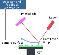


(1) : Cantilever, (2) : Support for cantilever, (3) : Piezoelectric element (to oscillate cantilever at its eigen frequency), (4) : Tip (Fixed to open end of a cantilever, acts as the probe), (5) : Detector of deflection and motion of the cantilever, (6) : Sample to be measured by AFM, (7) : xyz drive, (moves sample (6) and stage (8) in x, y, and z directions with respect to a tip apex (4)), and (8) : Stage.

(1) : Tip apex, (2) : Sample surface, (3) : Z-orbit of Tip apex, (4) : Cantilever.