Electron diffraction
[12]: Chpt 1,7,8 If instead of two slits there are a number of small points then similar phenomena can occur as shown in the second image where the wave (red and blue) is coming in from the bottom right corner.
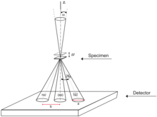
Close to an aperture or atoms, often called the "sample", the electron wave would be described in terms of near field or Fresnel diffraction.
[14] In 1650, Otto von Guericke invented the vacuum pump[15] allowing for the study of the effects of high voltage electricity passing through rarefied air.
[17] In 1869, Plücker's student Johann Wilhelm Hittorf found that a solid body placed between the cathode and the phosphorescence would cast a shadow on the tube wall, e.g.
In 1924 Louis de Broglie in his PhD thesis Recherches sur la théorie des quanta[5] introduced his theory of electron waves.
As stated by Louis de Broglie on September 8, 1927, in the preface to the German translation of his theses (in turn translated into English):[5]: v M. Einstein from the beginning has supported my thesis, but it was M. E. Schrödinger who developed the propagation equations of a new theory and who in searching for its solutions has established what has become known as “Wave Mechanics”.The Schrödinger equation combines the kinetic energy of waves and the potential energy due to, for electrons, the Coulomb potential.
Alexander Reid, who was Thomson's graduate student, performed the first experiments,[31] but he died soon after in a motorcycle accident[32] and is rarely mentioned.
[41] One significant step was the work of Heinrich Hertz in 1883[42] who made a cathode-ray tube with electrostatic and magnetic deflection, demonstrating manipulation of the direction of an electron beam.
To this day the issue of who invented the transmission electron microscope is controversial, as discussed by Thomas Mulvey[46] and more recently by Yaping Tao.
In 1931, Max Knoll and Ernst Ruska[39][40] successfully generated magnified images of mesh grids placed over an anode aperture.
[27][28] As early as 1929 Germer investigated gas adsorption,[56] and in 1932 Harrison E. Farnsworth probed single crystals of copper and silver.
John M Cowley explains in a 1968 paper:[64] Thus was founded the belief, amounting in some cases almost to an article of faith, and persisting even to the present day, that it is impossible to interpret the intensities of electron diffraction patterns to gain structural information.This has changed, in transmission, reflection and for low energies.
[92] The high-energy electrons interact with the Coulomb potential,[33] which for a crystal can be considered in terms of a Fourier series (see for instance Ashcroft and Mermin),[6]: Chpt 8 that is
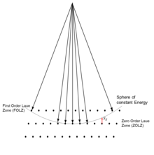
[98] For all cases, when the reciprocal lattice points are close to the Ewald sphere (the excitation error is small) the intensity tends to be higher; when they are far away it tends to be smaller.
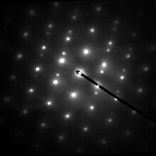
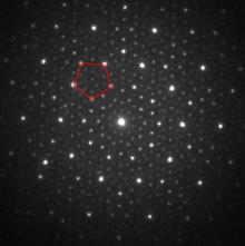
[1][2][4] A typical electron diffraction pattern in TEM and LEED is a grid of high intensity spots (white) on a dark background, approximating a projection of the reciprocal lattice vectors, see Figure 1, 9, 10, 11, 14 and 21 later.
For a more complete approach one has to include multiple scattering of the electrons using methods that date back to the early work of Hans Bethe in 1928.
[92] Even at very high energies dynamical diffraction is needed as the relativistic mass and wavelength partially cancel, so the role of the potential is larger than might be thought.
The position of Kikuchi bands is fixed with respect to each other and the orientation of the sample, but not against the diffraction spots or the direction of the incident electron beam.
[116] Different types of diffraction experiments, for instance Figure 9, provide information such as lattice constants, symmetries, and sometimes to solve an unknown crystal structure.
Unfortunately the method is limited by the spherical aberration of the objective lens,[7]: Chpt 5-6 so is only accurate for large grains with tens of thousands of atoms or more; for smaller regions a focused probe is needed.
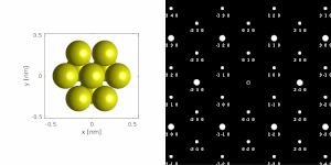
If a parallel beam is used to acquire a diffraction pattern from a single-crystal, the result is similar to a two-dimensional projection of the crystal reciprocal lattice.
From this one can determine interplanar distances and angles and in some cases crystal symmetry, particularly when the electron beam is down a major zone axis, see for instance the database by Jean-Paul Morniroli.
[139] Here the (220) are stronger bulk diffraction spots, and the weaker ones due to the surface reconstruction are marked 7 × 7—see note[d] for convention comments.
An extreme example of this is for quasicrystals,[140] which can be described similarly by a higher number of Miller indices in reciprocal space—but not by any translational symmetry in real space.
This can occur from inelastic processes, for instance, in bulk silicon the atomic vibrations (phonons) are more prevalent along specific directions, which leads to streaks in diffraction patterns.
[1]: Chpt 12 Often there is a probability distribution for the distances between point defects or what type of substitutional atom there is, which leads to distinct three-dimensional intensity features in diffraction patterns.
This integration produces a quasi-kinematical diffraction pattern that is more suitable[149] as input into direct methods algorithms using electrons[123][80] to determine the crystal structure of the sample.
An experimental diffraction pattern is shown in Figure 23 and shows both rings from the higher-order Laue zones and streaky spots.
The main uses of RHEED to date have been during thin film growth,[158] as the geometry is amenable to simultaneous collection of the diffraction data and deposition.
[167][168] As the Kikuchi lines carry information about the interplanar angles and distances and, therefore, about the crystal structure, they can also be used for phase identification[169]: Chpts 6–7 or strain analysis.