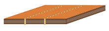
Planar transmission line
The earliest type of planar transmission line was conceived during World War II by Robert M. Barrett.
Their advantages depend on the exact types being compared, but can include low loss and a better range of characteristic impedance.
This method is particularly appealing for use with printed and integrated circuits because these structures can be manufactured with the same processes as the rest of the assembly simply by applying patterns to the existing substrate.
These include filters, power dividers, directional couplers, impedance matching networks, and choke circuits to deliver biasing to active components.
At the highest microwave frequencies planar transmission line types are generally too lossy and waveguide is used instead.
Because of this, ideal TEM transmission lines do not suffer from dispersion, a form of distortion in which different frequency components travel at different velocities.
Dispersion "smears out" the wave shape (which may represent the transmitted information) in the direction of the line length.
In a TEM line, discontinuities such as gaps and posts (used to construct filters and other devices) have an impedance that is purely reactive: they can store energy, but do not dissipate it.
These problems can be mitigated by using a high permittivity material as the substrate, which causes a higher proportion of the wave to be contained in the dielectric, making for a more homogeneous transmission medium and a mode closer to TEM.
The exact mode is identified by a pair of indices counting the number of wavelengths or half-wavelengths along specified transverse dimensions.
[13] Some planar types that are designed to operate as TEM devices can also support TE and TM modes unless steps are taken to suppress them.
High permittivity ceramic-PTFE laminates (e.g. Rogers Corporation 6010 board) are expressly intended for microwave applications.
[24] The electrical properties of the substrate of most interest are the relative permittivity (εr) and the loss tangent (δ).
The relative permittivity determines the characteristic impedance of a given line width and the group velocity of signals travelling on it.
A hard, rigid material such as quartz might be chosen as the substrate to avoid this problem, rather than an easier-to-machine board.
Suspended stripline is used in the mid microwave frequencies where it is superior to microstrip with respect to losses, but not as bulky or expensive as waveguide.
[37] The tendency of microstrip to radiate is generally a disadvantage of the type, but when it comes to creating antennae it is a positive advantage.
Trapped inverted microstrip shields the line on three sides preventing some higher order modes that are possible with the more open structures.
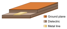
The return conductors are placed either side of the main line and made wide enough that they can be considered to extend to infinity.
On the other hand, the lack of ground planes means that the type is amenable to embedding in multi-layer structures.
A common way of manufacturing these is to take a thin sheet of metal with pieces cut out (typically, a series of rectangular holes) and insert this in the waveguide in much the same way as finline.
[70] At these frequencies it has a considerable advantage over microstrip for its low loss and it can be manufactured with similar low-cost printed circuit techniques.
A full waveguide solution for a complex design retains the low loss of air dielectric, but it would be much bulkier than finline and significantly more expensive to manufacture.
For instance Q factors in the thousands are theoretically possible but radiation from bends and losses in the dielectric-metal adhesive significantly reduce this figure.
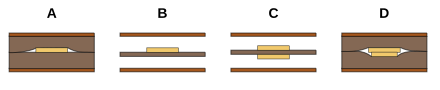
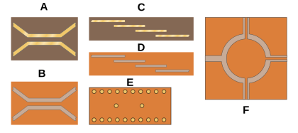
Example D in the diagram shows this kind of transition and features a balun consisting of a dielectric radial stub.
[91] The development of planar technologies was driven at first by the needs of the US military, but today they can be found in mass-produced household items such as mobile phones and satellite TV receivers.
As well as issuing contracts, Barrett encouraged research in other organisations, including the Airborne Instruments Laboratory Inc. (AIL).
[98] Finline, as a printed technology, is due to Meier in 1972,[99] although Robertson created finline-like structures much earlier (1955–56) with metal inserts.
It was quickly realised that the size of circuits could be hugely reduced by directly connecting components together with planar lines within the same housing.
In this technology, the planar transmission lines are directly incorporated in the semiconductor slab in which the integrated circuit components have been manufactured.