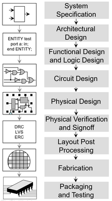
Integrated circuit design
ICs consist of miniaturized electronic components built into an electrical network on a monolithic semiconductor substrate by photolithography.
Analog design is more concerned with the physics of the semiconductor devices such as gain, matching, power dissipation, and resistance.
The design of some processors has become complicated enough to be difficult to fully test, and this has caused problems at large cloud providers.
The third step, physical design, does not affect the functionality at all (if done correctly) but determines how fast the chip operates and how much it costs.
[6] The use of standard cells allows the chip's design to be split into logical and physical levels.
Although the phases are presented here in a straightforward fashion, in reality there is iteration and these steps may occur multiple times.
The requirements are usually generated by a cross functional team that addresses market opportunity, customer needs, feasibility, and much more.
This involves low level definition and partitioning, writing code, entering schematics and verification.
After a design is created, taped-out and manufactured, actual hardware, 'first silicon', is received which is taken into the lab where it goes through bringup.
The result of the bringup phase is documentation of characterization data (how well the part performs to spec) and errata (unexpected behavior).
The process must be continually monitored and problems dealt with quickly to avoid a significant impact on production volumes.
Design at this stage is often statements such as encodes in the MP3 format or implements IEEE floating-point arithmetic.
At later stages in the design process, each of these innocent looking statements expands to hundreds of pages of textual documentation.
Using digital design components like adders, shifters, and state machines as well as computer architecture concepts like pipelining, superscalar execution, and branch prediction, RTL designers will break a functional description into hardware models of components on the chip working together.
To reduce the number of functionality bugs, a separate hardware verification group will take the RTL and design testbenches and systems to check that the RTL actually is performing the same steps under many different conditions, classified as the domain of functional verification.
The famous Pentium FDIV bug caused the results of a division to be wrong by at most 61 parts per million, in cases that occurred very infrequently.
Yet Intel was forced to offer to replace, for free, every chip sold until they could fix the bug, at a cost of $475 million (US).
[citation needed] RTL is only a behavioral model of the actual functionality of what the chip is supposed to operate under.
In practice there is not a straightforward progression - considerable iteration is required to ensure all objectives are met simultaneously.
Reuse of proven designs allowed progressively more complicated ICs to be built upon prior knowledge.
[15] The top-down design style makes use of optimization-based tools similar to conventional digital flows.
A challenge most critical to analog IC design involves the variability of the individual devices built on the semiconductor chip.
The underlying cause of this variability is that many semiconductor devices are highly sensitive to uncontrollable random variances in the process.