Nanometrology
Nanometrology has a crucial role in order to produce nanomaterials and devices with a high degree of accuracy and reliability in nanomanufacturing.
A challenge in this field is to develop or create new measurement techniques and standards to meet the needs of next-generation advanced manufacturing, which will rely on nanometer scale materials and technologies.
Anticipated advances in emerging U.S. nanotechnology industries will require revolutionary metrology with higher resolution and accuracy than has previously been envisioned.
It becomes important to measure the physical parameters so as to apply these phenomena into engineering of nanosystems and manufacturing them.
The measurement of length or size, force, mass, electrical and other properties is included in Nanometrology.
Various techniques based on physical phenomena have been developed which can be used for measure or determine the parameters for nanostructures and nanomaterials.
Nanotechnology is an important field because of the large number of applications it has and it has become necessary to develop more precise techniques of measurement and globally accepted standards.
The worldwide market for products with nanotechnology applications is projected to be at least a couple of hundred billion dollars in the near future.
[citation needed] Until recently, there almost no established internationally accepted standards for nanotechnology related field.
The International Organization for Standardization TC-229 Technical Committee on Nanotechnology recently published few standards for terminology, characterization of nanomaterials and nanoparticles using measurement tools like AFM, SEM, Interferometers, optoacoustic tools, gas adsorption methods etc.
At nanoscale while calibrating care needs to be taken for influence of external factors like vibration, noise, motions caused by thermal drift and creep, nonlinear behaviour and hysteresis of piezoscanner[2] and internal factors like the interaction between the artefact and the equipment which can cause significant deviations.
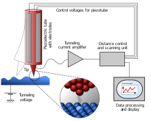
When a conducting tip is brought very near to the surface to be examined, a bias (voltage difference) applied between the two can allow electrons to tunnel through the vacuum between them.
Measurements are made by monitoring the current as the tip's position scans across the surface, which can then be used to display an image.
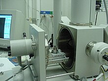
Another commonly used instrument is the scanning electron microscopy (SEM) which apart from measuring the shape and size of the particles and topography of the surface can be used to determine the composition of elements and compounds the sample is composed of.
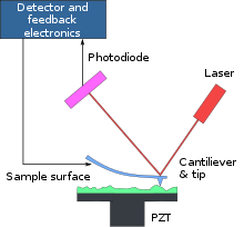
The instruments mentioned above produce realistic pictures of the surface are excellent measuring tools for research.
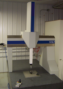
The probes for such a machine need to be small to enable a 3-D measurement of nanometre features from the sides and from inside like nanoholes.
The components of a nano CMM include nanoprobes, control hardware, 3D-nanopositioning platform, and instruments with high resolution and accuracy for linear and angular measurement.
At nanoscale a crystalline highly oriented pyrolytic graphite (HOPG), mica or silicon surface is considered suitable used as calibration artefact for achieving traceability.
Defining tolerances at nanoscale with suitable calibration standards for traceability is difficult for different nanomanufacturing methods.
There are a variety of nanostructures like nanocomposites, nanowires, nanopowders, nanotubes, fullerenes nanofibers, nanocages, nanocrystallites, nanoneedles, nanofoams, nanomeshes, nanoparticles, nanopillars, thin films, nanorods, nanofabrics, quantumdots etc.