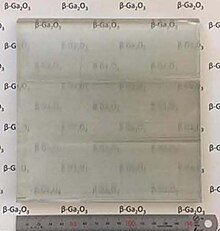
Gallium(III) oxide
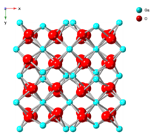
The β-phase’s bandgap of 4.7–4.9 eV and large-area, native substrates make it a promising competitor to GaN and SiC-based power electronics applications and solar-blind UV photodetectors.
[9] Ga2O3 exhibits reduced thermal conductivity and electron mobility by an order of magnitude compared to GaN and SiC, but is predicted to be significantly more cost-effective due to being the only wide-bandgap material capable of being grown from melt.
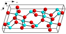
[34] ε-Ga2O3 films deposited by metalorganic vapour-phase epitaxy show a columnar structure with orthorhombic crystal symmetry.
[46][47] Since the first publication in January 2012 by the National Institute of Information and Communications Technology, in collaboration with Tamura Co., Ltd. and Koha Co., Ltd. of the world's first single-crystal gallium oxide (Ga2O3) field-effect transistors, the predominant interest in gallium oxide is in the β-polymorph for power electronics.
[48][7] Monoclinic β-Ga2O3 has shown increasing performance since 2012 approaching state of the art GaN and SiC power devices.
ε-Ga2O3 thin films deposited on sapphire show potential applications as solar-blind UV photodetector.