Etching (microfabrication)
[1]: 147 The wafer can be immersed in a bath of etchant, which must be agitated to achieve good process control.
Etching a thin layer of even a few micrometres will remove microcracks produced during backgrinding resulting in the wafer having dramatically increased strength and flexibility without breaking.
Some wet etchants etch crystalline materials at very different rates depending upon which crystal face is exposed.
[2] The authors employ multistream laminar flow that contains etching non-etching solutions to fabricate a glass groove.
The scanning electron microscopy (SEM) images demonstrate the breaking of the conventional theoretical limit of aspect ratio (width/height=0.5) and contribute a two-fold improvement (width/height=1).
KOH may introduce mobile potassium ions into silicon dioxide, and EDP is highly corrosive and carcinogenic, so care is required in their use.
Tetramethylammonium hydroxide (TMAH) presents a safer alternative than EDP, with a 37X selectivity between {100} and {111} planes in silicon.
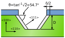
The {111}-oriented sidewalls have an angle to the surface of the wafer of: If the etching is continued "to completion", i.e. until the flat bottom disappears, the pit becomes a trench with a V-shaped cross-section.
If the original rectangle was a perfect square, the pit when etched to completion displays a pyramidal shape.
The plasma produces energetic free radicals, neutrally charged, that react at the surface of the wafer.
It bombards the wafer with energetic ions of noble gases, often Ar+, which knock atoms from the substrate by transferring momentum.
Because the etching is performed by ions, which approach the wafer approximately from one direction, this process is highly anisotropic.
Modern processes greatly prefer anisotropic etches, because they produce sharp, well-controlled features.