List of MOSFET applications
MOSFET scaling and miniaturization has been driving the rapid exponential growth of electronic semiconductor technology since the 1960s, and enable high-density integrated circuits (ICs) such as memory chips and microprocessors.
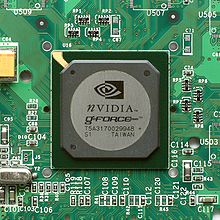
The MOSFET is the most widely used type of transistor and the most critical device component in integrated circuit (IC) chips.
[2] Planar process, developed by Jean Hoerni at Fairchild Semiconductor in early 1959, was critical to the invention of the monolithic integrated circuit chip by Robert Noyce later in 1959.
Atalla realised that the main advantage of a MOS transistor was its ease of fabrication, particularly suiting it for use in the recently invented integrated circuits.
These two factors, along with its rapidly scaling miniaturization and low energy consumption, led to the MOSFET becoming the most widely used type of transistor in IC chips.
The earliest experimental MOS IC to be demonstrated was a 16-transistor chip built by Fred Heiman and Steven Hofstein at RCA in 1962.
[17] In 1967, Bell Labs researchers Robert Kerwin, Donald Klein and John Sarace developed the self-aligned gate (silicon-gate) MOS transistor, which Fairchild Semiconductor researchers Federico Faggin and Tom Klein used to develop the first silicon-gate MOS IC.
[19] With its high scalability,[36] and much lower power consumption and higher density than bipolar junction transistors,[37] the MOSFET made it possible to build high-density IC chips.
The first multi-chip microprocessors, the Four-Phase Systems AL1 in 1969 and the Garrett AiResearch MP944 in 1970, were developed with multiple MOS LSI chips.
This isolation also makes it easier for the designers to ignore to some extent loading effects between logic stages independently.
Analog circuits depend on operation in the transition region where small changes to Vgs can modulate the output (drain) current.
Nevertheless, MOSFETs are widely used in many types of analog circuits because of their own advantages (zero gate current, high and adjustable output impedance and improved robustness vs. BJTs which can be permanently degraded by even lightly breaking down the emitter-base).
[vague] The characteristics and performance of many analog circuits can be scaled up or down by changing the sizes (length and width) of the MOSFETs used.
This means that complete analog circuits can be made on a silicon chip in a much smaller space and with simpler fabrication techniques.
Some ICs combine analog and digital MOSFET circuitry on a single mixed-signal integrated circuit, making the needed board space even smaller.
In the late 1980s, Asad Abidi pioneered RF CMOS technology, which uses MOS VLSI circuits, while working at UCLA.
In the case of a P-MOS, the body is connected to the most positive voltage, and the gate is brought to a lower potential to turn the switch on.
As it was fairly straightforward to fabricate a series of MOS capacitors in a row, they connected a suitable voltage to them so that the charge could be stepped along from one to the next.
[73] The CMOS active-pixel sensor was later developed by Eric Fossum and his team at NASA's Jet Propulsion Laboratory in the early 1990s.
[85] Advantages over bipolar junction transistors in power electronics include MOSFETs not requiring a continuous flow of drive current to remain in the ON state, offering higher switching speeds, lower switching power losses, lower on-resistances, and reduced susceptibility to thermal runaway.
[88] They are also widely used for MOS RF power amplifiers, which enabled the transition of mobile networks from analog to digital in the 1990s.
[95] LDMOS, a power MOSFET with lateral structure, is commonly used in high-end audio amplifiers and high-power PA systems.
[111] According to Colinge, numerous consumer electronics would not exist without the MOSFET, such as digital wristwatches, pocket calculators, and video games, for example.
Computers or telecommunication devices (such as phones) are not included here, but are listed separately in the Information and communications technology (ICT) section below.
[154] In 1967 the Texas Instruments Cal-Tech was the first prototype electronic handheld calculator, with three MOS LSI chips, and it was later released as the Canon Pocketronic in 1970.
[155] The first true electronic pocket calculator was the Busicom LE-120A HANDY LE, which used a single MOS LSI calculator-on-a-chip from Mostek, and was released in 1971.
[130] MOSFETs are commonly used for a wide range of audio-visual (AV) media technologies, which include the following list of applications.
This allows researchers to explore quantum effects by operating high-purity MOSFETs at liquid helium temperatures.
[239] In 1978, the Gakushuin University researchers Jun-ichi Wakabayashi and Shinji Kawaji observed the Hall effect in experiments carried out on the inversion layer of MOSFETs.
[241] In 1980, Klaus von Klitzing, working at the high magnetic field laboratory in Grenoble with silicon-based MOSFET samples developed by Michael Pepper and Gerhard Dorda, made the unexpected discovery of the quantum Hall effect.